

Flexible printed circuit boards (FPCs) have become the backbone of modern electronics—connecting sensors, modules, and displays inside smartphones, wearables, and medical devices. Unlike rigid boards, they can bend, fold, and twist to fit compact designs. But this flexibility introduces mechanical and thermal stress that, if mismanaged, leads to cracking, delamination, or electrical failure.
A single micro-crack in a flex layer can render a product useless. Therefore, understanding the causes of failure and how to prevent them is essential for design engineers and manufacturers seeking to meet high-reliability standards in dynamic applications.
The Challenges of Flexible PCB Design
Designing a flex PCB is far more complex than simply “making it bend.” It requires balancing electrical performance with mechanical durability. The key challenges include:
- Material Behavior under Stress
Polyimide films and copper foils deform differently under repeated bending. The designer must account for tensile and compressive stresses to prevent trace fatigue and micro-cracks. - Layer Stack-Up Complexity
Multi-layer flex and rigid-flex designs demand careful placement of stiffeners, coverlays, and adhesives. An improper stack-up can trap stresses or create uneven bend radii. - Miniaturization Pressure
As devices become thinner, flex regions are forced into tighter spaces, reducing the allowable bend radius and increasing the risk of copper fracture. - Thermal and Environmental Loads
Repeated exposure to heat, humidity, or chemical agents can accelerate delamination or oxidation, especially when the wrong materials or finishes are selected.
With these challenges in mind, let’s examine the 10 most common pitfalls that often lead to cracking and failure in flexible PCBs—and how to design against them.

10 Common Pitfalls That Lead to Cracking and Failure
1. Incorrect Material Selection
Material choice is the foundation of any reliable flex PCB design. Using inappropriate base films or copper types is a leading cause of cracking and premature failure.
Common Causes:
- Selecting stiff polyesters (PET) instead of flexible polyimide (PI) materials for dynamic flex regions.
- Using standard rolled-annealed (RA) copper for static applications where electro-deposited (ED) copper may perform better—or vice versa.
- Mismatched adhesives and coverlays that expand differently during thermal cycling.
Design Impact:
Incorrect material combinations cause micro-delamination between layers and reduced bend endurance. Over time, repeated flexing causes copper work-hardening, leading to trace fracture.
How to Avoid It:
- Choose polyimide base films (25–50 µm) for high-reliability and temperature stability.
- Match copper type to application: RA copper for dynamic flexing; ED copper for low-cost, static applications.
- Verify the coefficient of thermal expansion (CTE) compatibility among layers.
- Consult manufacturer datasheets or IPC-4202/4204 standards before finalizing materials.
- Include material stack-up documentation in the design package for supplier verification.
2. Improper Layer Stack-Up Design
Even when using quality materials, improper stack-up design can concentrate mechanical stress at weak points—especially in rigid-flex assemblies.
Common Causes:
- Placing copper layers asymmetrically relative to the neutral bend axis.
- Using unnecessary adhesive layers that increase stiffness in bend zones.
- Overlapping stiffeners or vias near flex transitions.
Design Impact:
Stress concentration leads to cracking at the rigid–flex interface or delamination between copper and dielectric layers. Asymmetrical stack-ups also cause unpredictable bend behavior, making assembly alignment difficult.
How to Avoid It:
- Keep symmetry around the neutral axis by evenly distributing copper layers.
- Use adhesiveless flex cores to improve flexibility and reduce stress buildup.
- Avoid placing vias or pads within 1.5 mm of bend lines.
- Maintain consistent stack-up documentation between design and manufacturing teams to ensure predictable bending characteristics.
- For multi-layer rigid-flex designs, simulate mechanical stress using tools like Ansys Mechanical or SolidWorks Simulation.
3. Ignoring Minimum Bend Radius Requirements
Bolded for featured snippet targeting:
The minimum bend radius defines how tightly a flexible PCB can bend without damaging the copper traces or dielectric layers. Ignoring this limit is the most common cause of cracking and open circuits in flex designs.
Common Causes:
- Designing bend radii smaller than the IPC-recommended ratio of 10× the flex thickness for single-sided circuits and 20× for multi-layer designs.
- Locating components or stiffeners too close to the bend zone.
- Failing to communicate bending specifications to assembly technicians.
Design Impact:
Too small a bend radius causes copper fatigue and delamination between copper and coverlay. Once the copper yields, it cannot recover, leading to early-life electrical failure.
How to Avoid It:
- Always calculate the minimum bend radius (Rmin) = k × total flex thickness, where k = 10–20 depending on layer count.
- Position stiffeners and connectors away from dynamic flex regions.
- Define bending direction and radius clearly in mechanical drawings.
- Use curved trace routing instead of sharp 90° angles to distribute stress evenly.
- Validate designs through dynamic flex testing (e.g., 10,000+ bend cycles).


4. Excessive Flexing Cycles Beyond Design Limits
Every flexible PCB has a finite bending life. Exceeding its rated number of flex cycles is a leading cause of copper fatigue and trace cracking. This issue often arises when a board intended for static flexing is used in dynamic applications.
Common Causes:
- Designing with standard copper foil instead of high-endurance RA copper for moving applications.
- Using tight bend radii in areas subject to repetitive motion.
- Failing to perform life-cycle testing during design validation.
- Ignoring the mechanical duty cycle of the final product (e.g., hinge mechanisms in foldable devices).
Design Impact:
Over time, repeated flexing causes work hardening in the copper, leading to micro-cracks that grow with each movement. Eventually, traces break, resulting in intermittent or complete circuit failure.
How to Avoid It:
- Identify whether the design is static-flex (bent once during assembly) or dynamic-flex (bent repeatedly during use).
- For dynamic-flex, use rolled-annealed (RA) copper with a high elongation rate.
- Apply strain relief features (curved traces, staggered routing) near bend zones.
- Conduct flex fatigue testing (typically 10,000–100,000 bend cycles).
- Maintain a bend radius ≥20× flex thickness for long-life flexing.

5. Unoptimized Manufacturing Processes
Even with an excellent design, manufacturing variations can introduce defects that weaken the flex area or compromise layer adhesion.
Common Causes:
- Excessive etching or plating stress that thins copper traces.
- Misaligned lamination leading to uneven adhesive flow.
- Over-curing coverlays or adhesives that make the flex region brittle.
- Improper handling during depanelization or stiffener attachment.
Design Impact:
Manufacturing-induced stresses lead to delamination, brittle flex sections, or cracking at the copper-to-dielectric interface. These issues often appear during final assembly or thermal cycling.
How to Avoid It:
- Choose manufacturers experienced with flex and rigid-flex PCB fabrication.
- Specify adhesiveless laminates and low-flow prepregs where possible.
- Communicate critical dimensions and bend locations clearly in Gerber and drawing files.
- Implement Design for Manufacturing (DFM) reviews with the fabrication partner.
- Include acceptance criteria per IPC-6013 (Qualification and Performance Specification for Flexible Printed Boards).

6. Improper Signal Path Routing and Sharp Trace Angles
Signal routing directly impacts both electrical integrity and mechanical durability. Poorly routed traces are a hidden cause of cracking and EMI issues.
Common Causes:
- Using 90° or acute trace corners in bend areas.
- Routing traces perpendicular to the bend line increases tensile stress.
- Inconsistent trace width or spacing near flex transitions.
- Neglecting controlled impedance in high-speed flex designs.
Design Impact:
Sharp trace corners act as stress concentrators, leading to copper cracking when the board flexes. In high-speed circuits, inconsistent trace geometry can also cause impedance mismatches, signal reflection, and EMI issues.
How to Avoid It:
- Route traces parallel to the bend axis where possible.
- Replace sharp corners with smooth arcs or teardrop transitions.
- Maintain uniform trace width and spacing to prevent stress risers.
- Use staggered trace routing for multi-layer flex to distribute strain.
- For high-speed applications, simulate impedance using tools like Polar Si9000 or Altium Designer’s Field Solver.
7. Lack of Stress-Relief Features in Design
Flex circuits require intentional design features to distribute mechanical stress evenly. Omitting these features often results in cracks near solder joints or copper pads.
Common Causes:
- Sudden transitions from rigid to flexible areas without gradual relief.
- Lack of strain-relief cutouts or fillets near connector pads.
- Overlapping stiffeners that restrict flex movement.
- Absence of coverlay openings in dynamic regions.
Design Impact:
Without stress relief, localized strain causes pad lifting, conductor fracture, or adhesive separation after repeated flexing. These failures may not appear immediately but can surface during reliability testing.
How to Avoid It:
- Add tear stops or relief slots at rigid-flex transitions.
- Use filleted pad shapes instead of square pads.
- Include flex relief zones in the mechanical outline.
- Employ progressive stiffeners that taper stiffness gradually.
- Run mechanical simulations to visualize stress distribution.

8. Poor Pad and Component Layout Near Bend Areas
Pad placement and component layout have a major influence on mechanical integrity. Placing components too close to a bend line can lead to solder joint cracking or pad delamination.
Common Causes:
- Locating SMD components or vias in flex zones.
- Using large copper pads near bends without fillets.
- Ignoring the neutral axis when placing heavy components.
- Overlapping stiffeners beneath flexing traces.
Design Impact:
When the PCB bends, solder joints near components experience tensile or compressive strain, resulting in joint cracking or lifted pads. Over time, this leads to intermittent electrical failure.
How to Avoid It:
- Maintain ≥3 mm clearance between components and bend areas.
- Position components along the neutral axis to minimize strain.
- Use curved fillets for all pad connections.
- Reinforce component regions with stiffeners if unavoidable.
- Avoid via-in-pad near bend regions to reduce stress transfer.
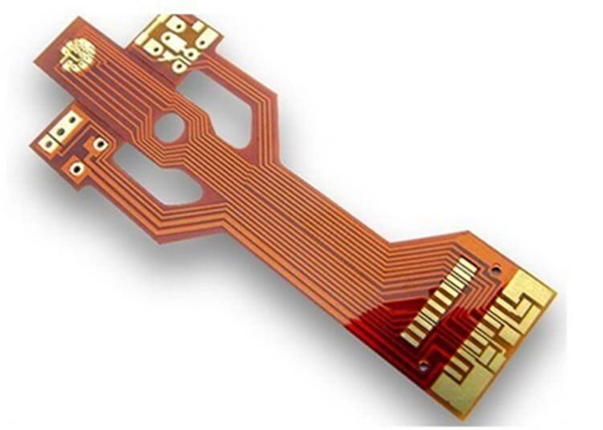
9. Ineffective Thermal Management Design
Flexible circuits dissipate heat less effectively than rigid boards, especially in thin polyimide layers. Poor thermal design increases the risk of delamination or copper oxidation.
Common Causes:
- Lack of thermal vias or heat-spreading planes.
- Over-concentrated power traces in narrow flex areas.
- High-current circuits without proper copper width.
- Poor airflow design in compact enclosures.
Design Impact:
Excessive heat accelerates adhesive degradation and layer separation. Thermal stress also expands copper differentially from the substrate, creating mechanical fatigue and cracks.
How to Avoid It:
- Add thermal vias and spreading planes near heat sources.
- Widen current-carrying traces to minimize Joule heating.
- Use copper-backed stiffeners or heat spreaders when necessary.
- Simulate heat flow using tools like Mentor FloTHERM or ANSYS Icepak.
- Specify high-temperature adhesive systems for power-flex designs.
10. Insufficient Testing and Quality Control
Even well-designed PCBs can fail if not properly tested or inspected during production. Lack of standardized testing allows hidden defects to reach assembly lines.
Common Causes:
- Skipping mechanical flex life testing or thermal cycling.
- Inadequate AOI (Automated Optical Inspection) for trace defects.
- Failure to conduct impedance or continuity testing after lamination.
- Poor documentation of acceptance criteria.
Design Impact:
Unverified boards can fail in the field due to latent cracks, poor adhesion, or electrical shorts, resulting in costly recalls and reliability issues.
How to Avoid It:
- Implement flex reliability tests (bend, torsion, and peel strength).
- Follow IPC-TM-650 for standardized testing procedures.
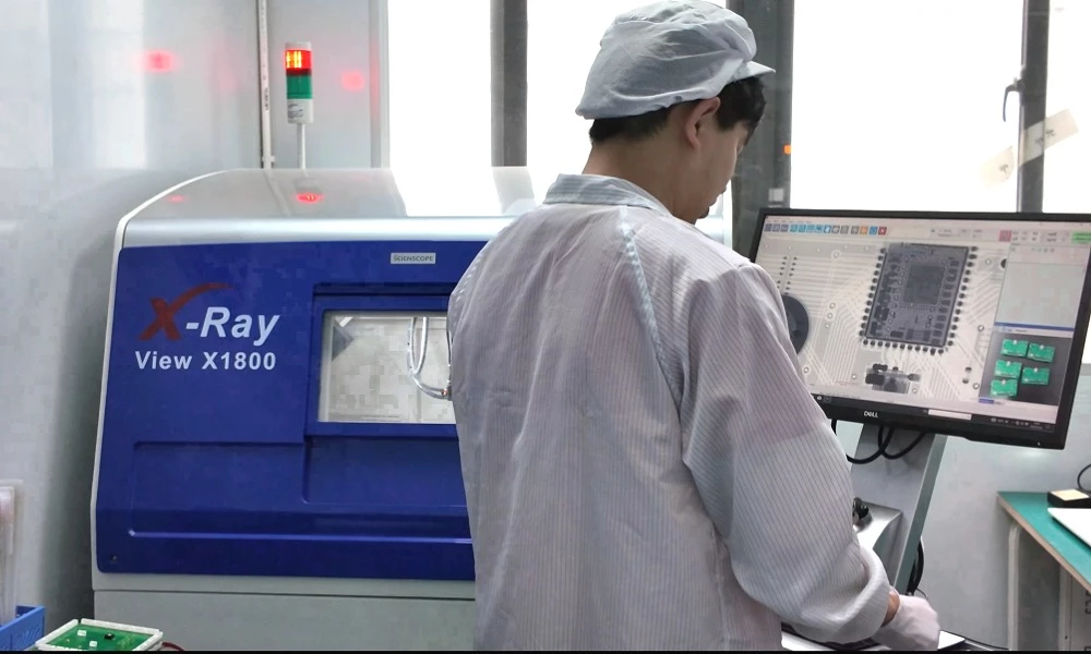
- Inspect solder joints and traces using 3D AOI or X-ray inspection.
- Maintain detailed QC documentation for traceability.
- Partner with suppliers who hold ISO 9001 or AS9100 certifications.

Summary:10 Common Flexible PCB Design Pitfalls and How to Avoid Them
| Common Design Pitfall | Cause / Description | Recommended Solution |
|---|---|---|
| Incorrect Material Selection | Using PET or mismatched copper types causes poor flexibility and adhesion. | Use polyimide base films and match RA or ED copper to application needs; verify CTE compatibility. |
| Improper Layer Stack-Up Design | Asymmetrical layers or excessive adhesives concentrate mechanical stress. | Follow the 10×–20× flex thickness rule, route curved traces, and define bend radius in drawings. |
| Ignoring Minimum Bend Radius | Bending below the safe radius causes copper fatigue and cracking. | Follow 10×–20× flex thickness rule, route curved traces, and define bend radius in drawings. |
| Excessive Flexing Cycles | Copper work-hardens under repeated motion, leading to fractures. | Use rolled-annealed copper, increase bend radius, and conduct cycle-life testing. |
| Unoptimized Manufacturing Process | Poor lamination, over-curing, or handling damage weakens flex zones. | Choose experienced flex PCB manufacturers, specify low-flow adhesives, and apply IPC-6013 controls. |
| Improper Signal Path Routing | Sharp corners and perpendicular traces amplify stress and EMI issues. | Route parallel to bend, use smooth arcs, maintain trace uniformity, and simulate impedance. |
| Lack of Stress-Relief Features | Missing fillets or relief zones cause pad lifting and copper cracks. | Add relief slots, fillets, and tapered stiffeners; simulate stress distribution. |
| Poor Pad & Component Layout | Components too close to bends create joint stress and pad detachment. | Keep ≥3 mm clearance, reinforce with stiffeners, and avoid vias in flex areas. |
| Ineffective Thermal Management | Heat buildup causes delamination and oxidation. | Add thermal vias, widen power traces, use copper-backed stiffeners, and simulate heat flow. |
| Insufficient Testing & Quality Control | Skipping flex and thermal testing allows hidden defects. | Perform bend/thermal tests, apply IPC-TM-650, and inspect with AOI/X-ray. |
Best Practices for Reliable Flex PCB Design
Designing a flexible PCB that endures mechanical stress while maintaining high electrical performance requires balancing innovation with proven engineering discipline. The following best practices combine insights from industry standards (like IPC-2223 and IPC-6013) and lessons learned from field failures.
1. Follow Rigid–Flex Design Rules
Rigid–flex assemblies integrate flexible interconnects between rigid sections. Each transition zone introduces potential stress concentration points.
Key Tips:
- Keep rigid-to-flex transitions smooth, avoiding 90° boundaries.
- Ensure layer count and copper thickness remain symmetrical about the neutral axis.
- Reinforce transition areas with progressive stiffeners or relief slots.
- Avoid vias in bending areas—place them in rigid zones where possible.
- Clearly define stack-up layers and materials in fabrication drawings.
2. Apply Proven Flex PCB Guidelines
Adhering to structured design standards is the simplest way to prevent mechanical and thermal failures.
Recommended Practices:
- Base every design on IPC-2223C Sectional Design Standard for Flexible Circuits.
- Follow minimum bend radius guidelines (10× for single-layer, 20× for multilayer).
- Avoid cross-hatching copper planes in high-current paths; instead, use continuous planes to reduce heating.
- Maintain consistent dielectric spacing across flex layers for predictable impedance control.
- Where multiple flex areas exist, define separate dynamic and static regions.
3. Collaborate Early with Manufacturers
Most flex failures occur when design assumptions don’t align with real-world fabrication processes. Early supplier involvement ensures manufacturability and repeatability.
Best Practices:
- Select experienced flex PCB fabrication partners (e.g., Sierra Circuits, Epec, or AdvancedPCB).
- Conduct Design for Manufacturing (DFM) reviews before releasing final Gerber files.
- Confirm minimum trace width, adhesive flow control, and stiffener placement tolerances.
- Request stack-up validation and material datasheets from the supplier.
- Build a prototype and perform bend and thermal cycling tests before full production.
4. Simulate Mechanical and Thermal Stress
Modern CAD tools allow engineers to simulate how the board behaves before physical prototyping.
Recommendations:
- Use finite element analysis (FEA) to model stress distribution along flex regions.
- Perform dynamic bending simulations to verify copper strain levels.
- Use thermal simulation software to confirm heat dissipation in power-flex designs.
- Validate the number of safe flex cycles under expected load conditions.
Simulations identify potential weak points early—saving time and avoiding costly redesigns later.
5. Prioritize Testing and Documentation
Even the best designs require validation. Consistent testing and documentation protect product reliability and ensure compliance with quality standards.
Checklist:
- Conduct mechanical bend testing to verify endurance life.
- Use AOI and X-ray inspection for detecting hidden cracks or delamination.
- Perform thermal cycling between –40°C and +125°C to check layer adhesion.
- Maintain detailed QC logs, inspection reports, and acceptance records per IPC-6013C.
- Include clear acceptance criteria and test reports in customer deliverables.
Conclusion
Avoiding the ten pitfalls outlined above is essential to achieving long-term reliability in flexible PCB designs.
By selecting the right materials, respecting bend radius limits, optimizing layout, and validating through testing, engineers can significantly reduce cracking and failure risks.
At IWDF Solutions, we help clients design and manufacture high-reliability flex and rigid–flex PCBs that meet the toughest performance requirements. Our one-stop service covers design consultation, prototyping, and volume production—ensuring your project succeeds from concept to completion.
(Contact us to discuss your next flex PCB design project.)
FAQs About Flexible PCB Cracking and Design Failures
1. What are the most common mistakes in flexible PCB design?
The most frequent issues include choosing incorrect materials, ignoring bend radius requirements, and placing components too close to flex zones. Poor signal routing and lack of stress relief are also leading causes of cracking.
2. How can I prevent cracking in flex circuits?
Use rolled-annealed copper, design with adequate bend radius, and include stress-relief features such as fillets and curved traces. Avoid over-flexing and ensure proper lamination during manufacturing.
3. What causes flexible PCBs to fail over time?
Flex PCBs typically fail due to material fatigue, thermal degradation, or stress induced during manufacturing. Inadequate testing or poor environmental resistance can also accelerate failure during product operation.
4. How can I improve flex PCB durability?
Follow IPC standards, choose adhesiveless laminates, and maintain symmetry in stack-up design. Validate every prototype with mechanical and thermal stress testing to confirm expected lifespan under real conditions.
5. What materials are best for high-flex applications?
High-endurance flex circuits use polyimide base films and rolled-annealed copper. For extreme conditions, specialized materials like liquid crystal polymer (LCP) may offer superior stability and moisture resistance.