

Modern vehicles rely on advanced printed circuit boards to manage power, control critical functions, and ensure safety. Whether you’re designing a battery management system for an EV, a motor controller for a hybrid, or an ECU for a conventional engine, your PCB must endure extreme temperatures, vibration, EMI, and moisture. Unlike consumer electronics, failures here can directly affect safety, performance, and trust.
This guide outlines key automotive PCB design guidelines—from component placement and thermal management to meeting industry standards. Aimed at PCB designers, supplier engineers, and OEM specialists, it offers practical advice for creating reliable, road-ready boards that strengthen your supply chain.
Where Are PCBs Used in Modern Vehicles?
Understanding the physical locations and operational environments of PCBs within a vehicle is fundamental to designing robust circuits. Different vehicle systems impose vastly different demands on PCB performance, thermal handling, and reliability expectations.
Powertrain and Engine Control Units (ECUs)
These are the core boards controlling propulsion. In electric vehicles (EVs), the traction inverter PCB converts DC battery power into AC power for the electric motor, managing high currents (often over 100 A) and voltages (typically 400–800 V). In traditional engines, the Engine Control Unit manages fuel injection, ignition timing, and emissions. Both operate in demanding conditions, requiring real-time processing, high reliability, and strong resistance to electrical noise.
Battery Management Systems (BMS)
A critical PCB in EVs and hybrids, the BMS monitors individual battery cell voltages (often 96–400 cells in series), temperatures, and overall current. It operates in high-temperature zones—sometimes near 60°C—and must detect faults within microseconds to ensure safety. These PCBs work with multiple voltage levels (high-voltage measurement, low-voltage control, and isolated communication), making electrical isolation and proper spacing between circuits vital safety requirements.
Onboard Chargers (OBC) and DC-DC Converters
In EVs and plug-in hybrids, the onboard charger converts AC mains power into DC to charge the high-voltage battery. These PCBs handle significant heat and require designs capable of managing high currents, often using specialized materials like metal cores or heavy copper. Similarly, DC-DC converters step down high-voltage battery power to 12 V for accessories and must maintain a stable output despite varying loads.
Advanced Driver Assistance Systems (ADAS)
ADAS relies on sensors like radar, LiDAR, and cameras, each containing specialized PCBs. For example, radar PCBs operate at high frequencies (e.g., 77 GHz) and require carefully controlled wiring, low-loss materials, and precise layout to maintain signal accuracy. Even minor interference can affect performance.
Infotainment and Instrument Clusters
Touchscreen displays, GPS modules, wireless connectivity (WiFi, 4G/5G, V2X), and multimedia processors live on infotainment PCBs. While less exposed to engine-bay extremes, these boards still endure vehicle vibration, temperature swings, and electromagnetic interference from adjacent power systems.
Body Electronics and Distributed Control Modules
Lighting control, HVAC, seat adjusters, door locks, and window motors all operate on network-distributed PCBs—some in exposed underbody locations, others in cabin-mounted electronics. These boards typically operate at 12 V or 48 V but must tolerate voltage transients, reverse polarity, and harsh moisture exposure.

Types of Automotive PCBs and Their Functions
The specific type of PCB you choose shapes every subsequent design decision. Material selection, layer count, and manufacturing process must align with the electrical and environmental demands of the application.
Rigid PCBs (FR-4 and High-Tg FR-4)
Standard FR-4 laminates (Glass Transition Temperature ~170°C) are cost-effective for many automotive applications. However, ICE engine bay applications and high-power EV systems often require High-Tg FR-4 (Tg ≥ 180–200°C) to resist warping during thermal cycling and to maintain dielectric strength at elevated temperatures. Most automotive ECUs and body control modules use rigid multilayer FR-4 or high-Tg FR-4 boards with 4–8 layers.
Metal-Core PCBs (MCPCB)
Aluminum or copper core laminates provide superior thermal conductivity compared to standard FR-4 (aluminum core: ~1.0 W/m·K versus FR-4: ~0.25 W/m·K). MCPCBs are essential for high-current, high-power applications like motor drivers, onboard chargers, and LED lighting control. The metal core acts as a built-in heatsink; designers route thermal vias directly from hot components to the aluminum base. The trade-off is cost and the requirement for careful electrical isolation between the thermal pad and power layers.
High-Density Interconnect (HDI) PCBs
ADAS modules, radar units, and high-frequency circuits demand fine-pitch routing, tight vias, and controlled impedance. HDI boards feature microvias (laser-drilled holes 0.1–0.2 mm diameter) stacked or staggered, often in a 1+N+1 or 2+N+2 configuration. This allows routing density necessary for BGA packages and high-speed differential pairs. HDI materials are often Rogers 4350, Taconic TLY, or high-Tg FR-4 with low-loss characteristics when impedance control is critical.
Rigid-Flex and Flex PCBs
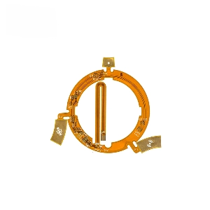
Applications requiring mechanical flex—airbag controllers, steering column electronics, folding mirror modules—use rigid-flex PCBs. These combine rigid and flexible regions on the same substrate, reducing connector count and improving mechanical reliability in areas subject to repeated bending. Rigid-flex designs require careful attention to bend radius (typically 10–15x the copper thickness) and via placement to prevent fatigue failure.


Component Placement, Routing, and Via Strategy in Automotive PCB Design
Designing an automotive PCB is fundamentally different from consumer electronics design. Every component placement decision, trace route, and via assignment must account for long-term reliability under thermal cycling, vibration, and electrical stress. Mistakes made during layout are exponentially more expensive to fix than mistakes caught during schematic review.
Component Placement: Thermal and Vibration Considerations
Begin your layout by dividing the board into functional zones: power delivery, analog measurement, digital processing, high-speed communication, and thermal hotspots. This zoning strategy minimizes noise coupling and simplifies thermal analysis.
Heat Generation and Dissipation
Power FETs, gate drivers, inductors, and transformers generate significant heat. Position these components near the board edge—preferably on the side facing a heatsink or natural airflow. Avoid placing them in corners where the copper area is limited and heat has nowhere to dissipate. For high-power boards, use thermal simulation tools (ANSYS Fluent, Icepak, or SIwave) to predict temperature distribution before finalizing layout.
In metal-core designs, thermal pads must be routed directly to the aluminum base with dense via arrays. Aim for at least 20–40 thermal vias under each power pad, sized to provide a thermal resistance of <0.5 °C/W per component. Standard via-to-via spacing should be 0.5–0.75 mm to avoid via-hole interference during plating.

Symmetrical Layout and Mechanical Stability
Thermal cycling causes repeated expansion and contraction—the mismatch between copper (CTE ~17 ppm/°C) and FR-4 (CTE ~13–15 ppm/°C) creates stress. Symmetrical layer stackups (e.g., 1oz-2oz-2oz-2oz-2oz-1oz copper distribution) minimize warping. Place large BGAs and heavy components centrally and symmetrically to distribute stress evenly.
In high-vibration environments (engine bay, near motor controllers), anchor mechanical supports using glue dots or solder anchors for tall components like electrolytic capacitors. Modern automotive standards often require mechanical vibration testing up to 20 G acceleration and thermal shock testing from -40°C to +125°C through 1,000 cycles per AEC-Q100 Grade 1 specifications.
Decoupling and Bypass Placement
Place decoupling capacitors as close as physically possible to IC power pins—not “approximately close” but measured in millimeters. A 100 nF ceramic capacitor intended to suppress high-frequency noise is useless if connected via a 10 mm trace; the trace inductance will dominate and mask the capacitor’s benefit.
For multilayer boards, use dedicated power and ground planes and stitching vias to create continuous, low-impedance power distribution networks. Every IC should have at least one local 100 nF ceramic within 5 mm of the power pin pair, plus regional 10–100 μF capacitors distributed across the board.

Trace Routing: Balancing Speed, Power, and EMC
In automotive designs, trace routing must simultaneously satisfy three conflicting demands: high-speed signal integrity, high-current power delivery, and electromagnetic compatibility.
High-Voltage and High-Current Routing
For power delivery paths handling 10+ A, use wide traces and multiple copper layers. A 10 A trace in standard 1 oz copper might require 150–200 mil width; in 2 oz copper, 100–125 mil. Always verify trace current capacity using IPC-2152 or manufacturer-specific calculators.
High-voltage traces (400 V, 800 V, or higher) demand strict adherence to creepage and clearance spacing. Creepage distance is the shortest distance along the board surface (including solder mask); clearance is the straight-line air gap. For a 400 V system in a polluted environment (Pollution Degree 3, typical for automotive):
- Clearance: 4.0 mm minimum (IEC 60664-1)
- Creepage: 8.0–12.8 mm, depending on insulation material group (basic isolation: 4 mm × 2 = 8 mm for reinforced isolation)
These distances must account for solder mask, conformal coating, and plating tolerances. Always add 0.5–1.0 mm margin beyond the minimum to account for manufacturing variation.

Signal Integrity and Impedance Control
High-speed automotive buses like Ethernet, CAN FD, and MIPI CSI/DSI require controlled impedance to prevent reflections and crosstalk. Use the following practices:
- Differential pairs (100 Ω differential impedance for Ethernet): maintain consistent trace width, spacing, and routing layer. Route both traces of a pair on the same layer and stay within ±5% length matching over the entire route.
- Single-ended high-speed signals (50 Ω for radar and sensor data): control trace width and distance to the nearest ground plane using stackup calculations.
- Reference planes: route high-speed signals adjacent to continuous ground planes. Avoid splitting ground planes directly beneath high-speed signals; if unavoidable, use stitching capacitors to bridge the gap.
Route high-speed traces on inner layers sandwiched between ground planes whenever possible. This provides electromagnetic shielding and maintains consistent return paths. Avoid routing near board edges; radiation from edge vias and traces can violate EMC limits.
EMI/EMC Layout Techniques
Electromagnetic interference is a primary failure mode in automotive electronics. To minimize EMI:
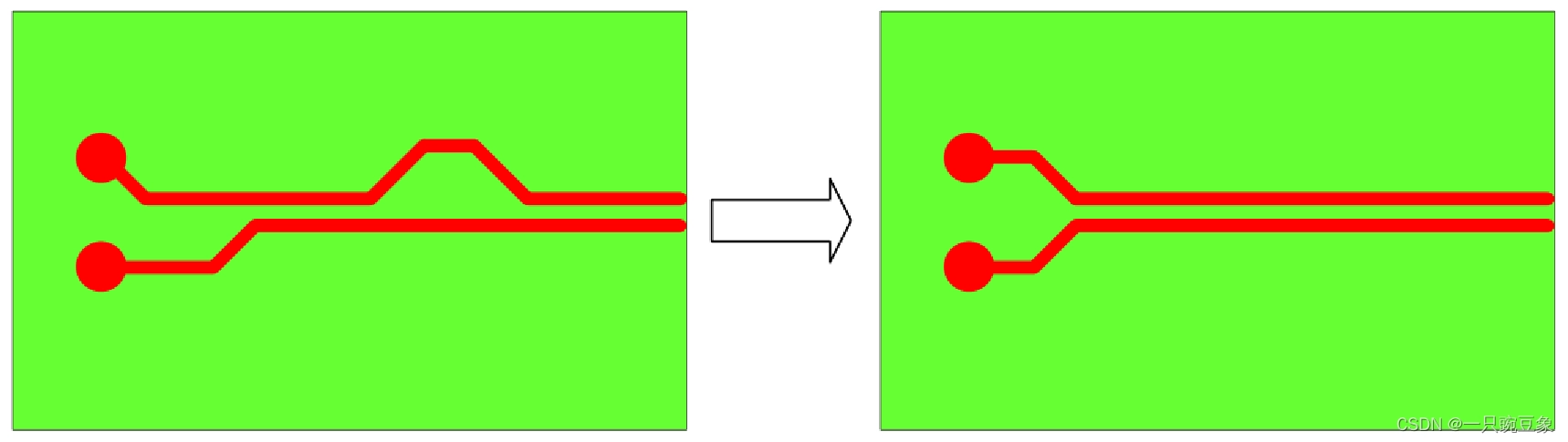
- Avoid 90-degree trace corners: use 45-degree miters or curves to reduce reflections and radiation.
- Minimize loop areas: route signal and return paths in parallel; never spread them across distant areas of the board.
- Ground stitching vias: Place vias every 5–10 mm around the perimeter of the board and around shielded regions to contain electromagnetic radiation.
- Separate analog and digital circuits: use physically distinct regions and a single-point ground connection (star grounding) to avoid ground loops.
- High-current switching near fast transients: group MOSFET gates, drivers, and their bypass capacitors in tight clusters to minimize loop inductance. A switching FET with poor decoupling creates dV/dt that radiates as wideband EMI.

Stackup Design: The Backbone of Reliable Automotive PCBs
A well-planned layer stackup is the foundation of signal integrity, thermal management, and EMC performance. Poorly chosen stackups lead to crosstalk, thermal runaway, and EMI failures that cannot be fixed in software.
Typical Automotive Stackup Examples
6-Layer Mixed-Signal Board (ECU, BMS, or Infotainment)
textL1: Signals + High-Speed (0.5 oz or 1 oz)
L2: Ground Plane (solid, 1 oz)
L3: Power + Signals (1 oz or 2 oz)
L4: Power Plane (1 oz or 2 oz, split permitted for isolated domains)
L5: Ground Plane (solid, 1 oz)
L6: Low-Speed I/O + Debug (0.5 oz or 1 oz)
This stackup maintains tight coupling between L1-L2 and L5-L6 for signal-ground return pairs. Prepreg thickness between layers should be chosen to achieve the desired impedance; typically 2–3 mil prepreg for 50 Ω single-ended and 100 Ω differential pairs.

8-Layer High-Power Board (Motor Driver, Onboard Charger)
textL1: Gate Drivers + Control Signals (0.5 oz)
L2: Ground (solid, 2 oz)
L3: Power Input / Output (2–3 oz)
L4: Thermal / Copper Pour (2–3 oz)
L5: Isolated Secondary (2–3 oz, if transformer-isolated)
L6: Ground (solid, 2 oz)
L7: Control Circuits (1 oz)
L8: Ground + Thermal Return (2 oz)
Heavy copper in L3-L5 spreads current and heat. L4 may be partially solid copper with carefully designed islands for thermal spreading, even if electrically isolated. L8 provides a thermal return path for components mounted on the bottom side.

10-Layer ADAS/Radar Board (Controlled Impedance + RF)
textL1: RF Traces / Antenna Feed (0.5 oz)
L2: Ground (solid, 0.5 oz, lossy material for broadband absorption)
L3: Mixed Signal (high-speed differential pairs)
L4: Ground (solid, 0.5 oz)
L5: Digital + Control (1 oz)
L6: Power (1 oz, split if needed)
L7: Ground (solid, 1 oz)
L8: Low-Speed I/O (1 oz)
L9: Power Return (1 oz)
L10: Ground (solid, 1 oz)
RF-focused boards often use Rogers 4350, Taconic TLY, or Arlon 25N for low-loss dielectric. L2 may use lossy material to absorb reflections in broadband radar applications. Tight control of dielectric constant (Dk ±5%) across all layers is essential.
Symmetry and Balanced Construction
All stackups should follow the symmetry rule: mirror layer thickness and material composition about the board centerline. A board with 2 oz copper on L1 and 1 oz on L8 will bow during reflow; the asymmetric stress during manufacturing carries forward into service life, eventually causing solder joint failures.
Calculate your stackup early using laminate design software provided by materials suppliers (Isola, Rogers, Panasonic, Nelco). Account for copper foil thickness, prepreg resin content, and resin fill to predict finished dielectric thickness.
How EV, Hybrid, and ICE Vehicle Conditions Shape PCB Design Strategy
The operating environment and electrical architecture of each vehicle type demand specific design prioritization. A layout that excels in an ICE engine bay may fail in an EV high-voltage system, and vice versa.
Electric Vehicles (EVs): High-Voltage Isolation and Thermal Management
EV powertrains introduce unprecedented challenges. High-voltage systems operating at 400–800 V create arc and creepage risks that must be engineered out of every design. Additionally, the power density of traction inverters and onboard chargers generates heat that, if mismanaged, can accelerate component aging or trigger thermal runaway in adjacent systems.
Isolation Coordination: Reinforced isolation (2× creepage and clearance) is mandatory between high-voltage power circuits and low-voltage control/measurement circuits. The reinforced insulation must be substantiated through design calculation per IEC 60664-1, physical separation, and conformal coating. A single solder bridge or conductive contamination in a high-voltage area can fail a board instantly.
Thermal Modeling: EV boards demand thermal simulation before layout finishes. Use boundary conditions matching the vehicle platform: ambient air temperature 25–60°C, depending on mounting location, natural or forced convection, depending on proximity to cooling ducts. Identify hotspots—any component exceeding 125°C under worst-case ambient—and redistribute copper, add thermal vias, or specify a lower-power variant.
Material Selection: High-Tg FR-4 (Tg ≥ 180°C) is the minimum; many automotive suppliers now specify polyimide or FR-408HR (Tg ≈ 200°C) for additional headroom. Higher-Tg materials better resist glass transition effects and CTE mismatch during thermal cycling. For thermal-critical applications, consider aluminum metal-core laminates with thermal conductivity up to 2 W/m·K.
Power Distribution: Thick copper (2–3 oz or heavier) with wide traces minimizes I²R losses and voltage drop. In a motor inverter, every 100 mV of voltage drop between the battery and gate driver increases switching losses and heating. Parallelize current paths; never use a single trace for 200 A.
Hybrid Vehicles: Dual-Domain Isolation and Noise Management
Hybrids operate two simultaneous power systems—12/48 V conventional and 200–400 V high-voltage traction. The challenge is preventing cross-domain interference while managing the complexity of dual domains.
Physical and Electrical Separation: Use moats (routed slots in copper planes) or PCB cutouts to physically isolate high-voltage and low-voltage sections. Route a low-impedance ground connection at a single point (star grounding) to prevent ground loops, then isolate all signal paths using opto-isolators or isolated gate drivers.
EMC Complexity: The high dV/dt and high dI/dt switching transients in the high-voltage converter couple capacitively and inductively into low-voltage measurement circuits. Without careful shielding, the battery voltage measurement (typically ±10 mV accuracy) will be destroyed by crosstalk. Use Faraday cages around low-voltage analog circuits and route their return paths directly to the star ground point.
Component Mixing: Never place 12 V consumer-grade components immediately adjacent to 400 V power FETs. The thermal environment differs dramatically, and the noise floor is 100× higher. Separate them by at least 10 mm and use shielded enclosures if space permits.
Internal Combustion Engine (ICE) Vehicles: Vibration, Temperature, and Mechanical Robustness
ICE engine bay PCBs endure the harshest automotive environment. Temperatures swing from -40°C in winter to +125°C sustained operation within centimeters of the exhaust manifold. Vibration from engine combustion reaches 10–20 G peaks, and corrosive oils and coolant can damage solder joints over time.
CTE Management: FR-4’s Z-axis CTE (~17 ppm/°C) is high; when thermally cycled -40 to +125°C repeatedly, plated through-hole barrels experience > 3% diameter change relative to the copper pad. The result: pad cratering and barrel cracks. Use high-Tg materials with lower CTE, maintain symmetrical stackups, and perform thermal cycling validation per AEC-Q100 (1,000 cycles minimum).
Vibration Withstand: Heavy components (electrolytic caps, inductors, transformers) need mechanical support. Apply a polyimide or epoxy glue dot under the component body, not just solder. Design the PCB footprint with anchor pads on opposite corners. In critical applications, add mechanical clips or standoffs.
Conformal Coating: Engine bay boards must be coated to resist moisture ingress and corrosion. Apply silicone-based conformal coatings (Parylene, silicone, urethane) with a thickness of 25–75 μm over all traces, pads, and solder joints. For high-voltage boards, select coatings with high dielectric strength (>20 kV/mm) and validate surface insulation resistance (SIR) per IPC-TM-650 2.3.28 after salt fog exposure.
Pad and Via Design for ICE: ICE boards often use older plating technologies (electroless copper, bright tin, lead-free HASL) that degrade faster than modern ENIG. Design with larger annular rings (6–7 mils for Class 3 instead of 5 mils) and avoid via-in-pad where possible; the stress relief is not worth the future reliability risk.
Thermal Design: Managing Heat in High-Power Automotive PCBs
Thermal failure is one of the leading causes of automotive PCB recalls. A board that operates at safe temperatures during bench testing may fail within months in a vehicle if thermal design is neglected.
Thermal Via Design and Placement
Thermal vias transfer heat from a component’s thermal pad (typically under a power FET or power IC) to internal copper layers or heatsinks. The effectiveness of thermal vias depends on:
- Number of vias: More is better, but diminishing returns appear after 20–40 vias per pad.
- Via diameter: Smaller vias (10–12 mil) offer more quantity per area but require finer drilling; 12–15 mil vias balance manufacturability and density.
- Spacing: 0.5–0.75 mm pitch avoids via-hole plating defects.
- Target layers: Route thermal vias to internal ground planes (typically L2 and L5 in a 6-layer board), then use copper pours on those planes to spread heat horizontally.
A typical thermal via array under a 25×25 mm MOSFET pad might use 36–40 vias in a 6×6 or 6×7 grid, reducing thermal resistance from the component to the internal plane from ~2–3 °C/W down to 0.3–0.5 °C/W.

Copper Thickness and Thermal Spreading
Internal plane copper thickness directly impacts heat spreading. Compare thermal performance:
- 1 oz copper (1.4 mil): baseline, lowest cost; acceptable for < 50 W boards.
- 2 oz copper (2.8 mil): standard for most automotive boards; provides ~2× the thermal spreading.
- 3–4 oz copper (4.2–5.6 mil): specified for motor drivers, converters, and boards dissipating >100 W in confined areas.
In a motor driver dissipating 200 W, the thermal path is: FET junction → die attach → copper pad → thermal vias → internal plane → board edge or heatsink. Each step has thermal resistance; the sum must be low enough to keep the FET junction < 150°C (typically derated 20–30% from absolute maximum).
Use thermal simulation to size copper thickness. Input the component’s thermal pad dissipation, ambient temperature, and heatsink specification, then iterate on copper thickness until the simulation predicts acceptable temperatures.

Heatsink Integration and Substrate Options
For high-power applications, attach an external aluminum heatsink to the board’s back side or to the component itself. Calculate required heatsink surface area using:
Rth,heatsink=PdissipatedTjunction−Tambient−Rth,junction−to−case−Rth,case−to−board
Solve for the allowable heatsink thermal resistance, then select a heatsink with that rating.
For extreme cases (inverters, onboard chargers >5 kW), specify a metal-core PCB with direct heatsink attachment. The aluminum core provides 2–4 °C/W lower thermal resistance than FR-4 with vias.
Designing for Reliability: EMI, Thermal Cycling, and Environmental Stress
Reliability is not a feature—it is a mandate in automotive. Boards must withstand 200,000+ kilometers of operation, spanning 15+ years and 10,000+ thermal cycles.
EMI and EMC Compliance
Automotive EMC testing is rigorous. Typical standards include:
- CISPR 25: Emissions up to 150 MHz; limits typically 40 dBμV/m @ 10 m.
- ISO 11452-x: Immunity testing for RF, conducted transients, and electrostatic discharge.
- IEC 61000-4-x: Additional immunity tests (surge, burst, etc.).
Layout techniques to meet EMC:
- Ground planes: Use solid, continuous ground planes on at least 2–3 inner layers. Avoid splits; if necessary, bridge splits with stitching capacitors placed within 5 mm of the signal trace crossing.
- Stitching vias: Place vias every 5–10 mm around the board perimeter and around sensitive signal regions. This creates a Faraday cage, confining radiation. For high-frequency designs (77 GHz radar), reduce spacing to 2–3 mm.
- Differential signaling: CAN, Ethernet, MIPI CSI/DSI, and LIN interfaces should use differential pairs routed with matched length, tight spacing, and a solid ground reference layer adjacent.
- Ferrite beads and filters: Place ferrite beads on antenna feeds, crystal oscillator connections, and any trace exiting the shielded region. Use integrated LC filters for power supply lines entering the board.
- Component placement isolation: Keep switching power supplies, motor drivers, and high-current paths far from sensitive analog circuits (ADCs, op-amps). If separation is impossible, use shielded enclosures or guard traces.
Thermal Cycling and CTE Mismatch
Thermal cycling is the primary acceleration factor for solder joint fatigue. A board experiencing -40 to +125°C, 1,000 times, must maintain mechanical integrity of every via and solder joint.
Design strategies:
- Symmetrical stackup: ensures uniform expansion and minimizes warping.
- Material matching: select laminates with CTE-matched copper foil and resin. High-Tg materials (polyimide, FR-408HR) have lower Z-axis CTE than standard FR-4.
- Micro-vias for critical nets: blind and buried vias reduce stress concentration compared to through-holes spanning many layers.
- Stress relief: PCB cutouts or “fuses” in large copper planes allow localized expansion without cracking the board.
Validate thermal cycling performance using mechanical simulation (ANSYS, COMSOL) or accelerated physical testing per AEC-Q100-011 (thermal cycling, -40 to +125°C, 500–1,000 cycles).
Moisture and Corrosion Protection
Engine bay PCBs are exposed to humidity, salt spray, and condensation. Without protection, copper traces oxidize, solder joints re-wet, and insulation resistance drops.
Conformal coatings:
- Acrylic: low cost, moderate protection; suitable for protected interior locations.
- Urethane: better moisture resistance; faster cure time.
- Silicone: best high-temperature stability; preferred for engine bay; higher cost.
- Parylene: hermetic encapsulation via vapor-phase deposition; excellent for high-reliability applications but expensive.
Apply coating uniformly to all surfaces, 25–75 μm thickness. Verify that masked areas (connectors, test points) are adequately protected. Perform SIR testing after salt fog exposure to ensure long-term reliability.
Surface finish selection:
- ENIG (Electroless Nickel, Immersion Gold): best overall; 3–5 μm nickel + 0.05–0.1 μm gold. Excellent corrosion resistance and long shelf life. Standard for automotive.
- HASL (Hot Air Solder Leveling): cost-effective but variable thickness; older designs; less common in high-reliability automotive.
- OSP (Organic Solderability Preservative): thin organic coating; excellent solderability; moderate shelf life; suitable for boards with conformal coating.
For high-voltage boards, ENIG is preferred because the nickel barrier prevents copper migration through the gold layer, maintaining insulation resistance over time.

Automotive Standards: IPC, ISO, and AEC Compliance Explained
Compliance with automotive standards is not optional; it is a contractual requirement for Tier-1 and OEM supply. These frameworks define what “safe and reliable” means and how to prove it.
IPC-2221: Generic PCB Design Standard
IPC-2221 establishes minimum design rules for spacing, trace widths, via dimensions, and material selection. Key automotive-relevant rules:
Conductor spacing (IPC-2221A, Table 2-1):
For voltage potentials between adjacent conductors:
- ≤50 V: 0.005″ (0.13 mm) minimum
- 50–100 V: 0.01″ (0.25 mm) minimum
- 100–200 V: 0.02″ (0.5 mm) minimum
- 200 V: refer to IEC 60664-1 for creepage/clearance calculations
For automotive high-voltage applications (400 V, 800 V), use IEC 60664-1 instead; IPC-2221 is insufficient.
Via design:
- Annular ring (copper area surrounding the drilled hole): minimum 0.005″ (0.13 mm) for Class 2, 0.0079″ (0.2 mm) for Class 3 (external layer).
- Via hole size: 8–15 mil diameter common; smaller vias allow higher density but require tighter process control.
- Aspect ratio (hole depth : diameter): maintain below 10:1 to ensure uniform plating and mechanical reliability.
Calculate your via land size using: Land diameter = Hole diameter + 2(Annular ring) + 2(Fabrication tolerance)
For a 12 mil via with 5 mil annular ring and ±4 mil tolerance: Land = 12 + 2(5) + 2(4) = 30 mil.
Trace width for current:
IPC-2152 provides detailed charts. As a rule of thumb, 1 oz copper traces supporting 1 A require ~8 mils width; 2 oz copper requires ~5 mils. For power delivery in EVs, use 2–3 oz copper and calculate explicitly.
IPC-6012 and IPC-6012DA: Rigid PCB Qualification Standard
IPC-6012 classifies rigid PCBs into three reliability classes:
- Class 1: General-purpose consumer electronics.
- Class 2: Dedicated service equipment and commercial products.
- Class 3: High-reliability products, e.g., automotive, medical, aerospace.
Automotive PCBs must meet Class 3 as a baseline. Class 3 requirements include:
- Annular ring: minimum 0.002″ (0.051 mm) internal, 0.004″ (0.1 mm) external after all processes.
- Solder mask thickness: 0.001–0.004″ (25–100 μm) depending on conductor spacing.
- Hole wall plating: minimum 0.8–1.0 mil for through-holes.
- Copper pattern limits: ±75 μm on boards up to 300 mm, ±150 μm on boards to 600 mm.
- Delamination test: <5% weight loss after IPC-TM-650 2.3.3.
- Thermal cycling: 1,000 cycles -40 to +125°C without electrical failure (functional test required).
IPC-6012DA is the automotive revision, adding requirements for vehicle-specific conditions like vibration testing and higher reliability acceptance criteria.
ISO 26262: Functional Safety Standard
ISO 26262 is the gold standard for automotive functional safety—the framework ensuring that even when a component fails, the system enters a safe state and does not cause harm.
ASIL levels:
- ASIL D (Automotive Safety Integrity Level D): Highest risk; failure could result in fatality or severe injury.
- ASIL C: Serious injury possible.
- ASIL B: Minor injury or temporary incapacity.
- ASIL A: Low risk; inconvenience or discomfort.
PCB designers contribute to functional safety by:
- Design redundancy: Critical circuits (braking, steering, high-voltage monitoring) use dual sensors and logic to detect and isolate failures.
- Diagnostic coverage: Watchdog timers, parity checks, and self-test functions detect faults within milliseconds.
- Safe failure modes: When faults occur, the board must enter a known safe state (e.g., disable motor drive, activate emergency braking).
- Isolation zones: High-voltage and low-voltage circuits are physically and electrically isolated; failure in one cannot cascade to the other.
PCB-level contributions to ISO 26262 compliance:
- Reserve test points for diagnostic circuits to measure critical voltages.
- Implement watchdog circuits with dedicated traces to independent shutdown logic.
- Use dual ground planes with isolated return paths for high-voltage circuits to prevent fault propagation.
- Design redundant current-sensing circuits where necessary.
While ISO 26262 is a system-level standard, PCB designers must understand ASIL requirements and design boards that enable diagnostic and redundancy features.
AEC-Q100 / Q200: Component Qualification Standards
AEC-Q100 qualifies semiconductor components for automotive use; AEC-Q200 qualifies passive components. While not directly a PCB standard, these specifications influence PCB design through thermal and reliability requirements.
AEC-Q100 Grade 1 components are rated to 125°C junction temperature continuously. A designer specifying such parts must ensure the PCB layout maintains the component below 125°C. This creates a feedback loop: if thermal simulation predicts 135°C, you must increase copper area, add heatsinks, or select lower-power components.
Derating rules:
- Specify components for 20–30% derated operation (e.g., 100 mA resistor used at 70–80 mA).
- Use Grade 1 (automotive-qualified) components; consumer-grade parts will fail prematurely in vehicle environments.
- Verify junction temperature under worst-case ambient (60°C for underbody, 85°C for near exhaust).

Design for Manufacturability (DFM) and Assembly (DFA): Bridging Design and Production
An elegant design that cannot be manufactured reliably is worthless. Engaging with your PCB manufacturer early in the design phase prevents costly spins and schedule delays.
Key DFM Considerations
Component Footprints and Solderability
Use IPC-7351 standard footprints; avoid custom footprints unless absolutely necessary. Verify that all pads accommodate the component lead size with adequate solder fillet area. For BGAs, use via-in-pad with copper-filled vias and solder-mask tenting to improve thermal performance without creating solder voids.
Panelization and Manufacturability
Design your board to panelize efficiently. Include v-score lines or tab routes between adjacent board copies to enable automated depanelization. Leave at least 5–10 mm margin around the outer edge for process fiducials and registration marks.
Trace and Space Design Rules
Coordinate with your manufacturer’s minimum trace width, space, and via capabilities. High-volume automotive often uses:
- Minimum trace width: 4–5 mils
- Minimum space: 4–5 mils (between copper-to-copper)
- Via capture pad: 12 mils minimum diameter
- Annular ring: 5–7 mils (Class 3)
If your schematic requires 2-mil traces due to routing density, consult with the manufacturer—you may need to accept longer lead times and higher cost, or re-route using 4–5-mil traces.
Solder Mask and Silkscreen
Automotive boards often specify liquid photoimageable (LPI) solder mask for better definition and reliability than dry-film. Avoid solder mask over vias that will be underfilled (risk of solder voids). For test points, use tented vias with small openings to guide probe contact but prevent solder wicking.
Test Points and In-Circuit Test (ICT)
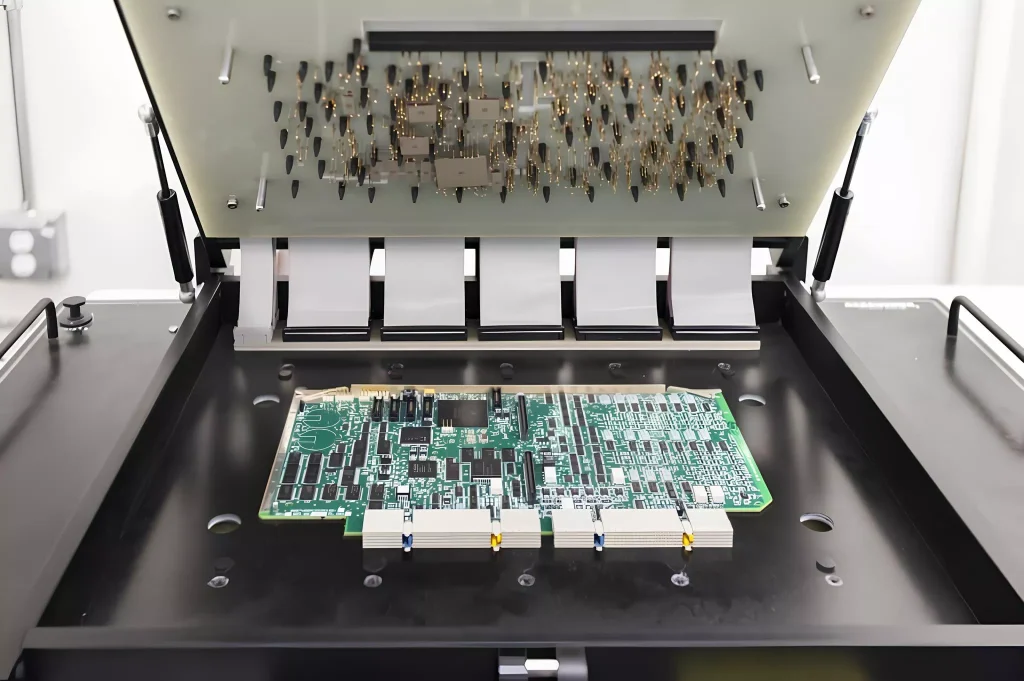
Reserve dedicated test points for critical nets: power rails, ground, high-speed clocks, analog measurement lines, and diagnostic signals. Arrange test points in a grid pattern compatible with your test equipment’s probe spacing (typically 50 or 100 mil pitch for ICT).
For automotive boards, functional testing is mandatory; ICT alone is insufficient. Design boards with self-test capabilities: JTAG/boundary scan for digital circuits, ADC self-calibration, and diagnostic read-back registers to verify DSP operation.
DFA: Assembly Ease Checklist
Component orientation:
All resistors, capacitors, and passive components should be oriented consistently (same rotation). This accelerates visual inspection and rework.
Large component placement:
Place heavy components (inductors >1 μH, large electrolytic caps) on the primary assembly side (top) if possible, avoiding bottom-side placement that complicates fixture design and increases rework time.
Thermal design and assembly:
If using conformal coating, specify selective coating to avoid coating connectors, test points, and areas requiring rework. Coordinate coating process with assembly to prevent flux residue under the coating.
Mixed-technology assembly:
Separate through-hole and surface-mount components to simplify the assembly sequence. If through-hole components are necessary, place them after solder reflow to avoid thermal stress.
When to Involve Your PCB Manufacturer in Automotive Projects?
Many design problems are cheaper to fix in schematic or early layout than in prototype or production. Engaging your automotive PCB manufacturer early unlocks their process expertise and prevents surprises.
Design Consultation Phase
Before layout begins, send your manufacturer:
- Preliminary schematic with estimated layer count, voltage levels, and current.
- Component list with package types (BGA pitch, number of pins, thermal pad size).
- Environmental specification: operating temperature, vibration profile, and humidity class.
- Compliance requirements: standards (IPC-6012 Class 3, AEC-Q, ISO 26262 ASIL level).
Your manufacturer can advise on:
- Stackup options: material, copper weight, prepreg thickness for impedance control.
- Manufacturing constraints: minimum trace/space, via capture pad sizes, and plating limitations.
- Cost-optimization: suggestions to reduce layer count, material cost, or special processes without compromising reliability.
Design Review Phase
Once the layout is 70–80% complete, schedule a formal design review with your manufacturer. Send:
- Schematic (for reference)
- PCB layout in Gerber format
- Bill of materials with component datasheets
- Design specifications: creepage/clearance requirements, impedance targets, thermal budget
A automotive PCB manufacturer review typically identifies:
- Design rule violations: traces too thin, vias too close to pads, and silk-screen overlap issues.
- Manufacturing risks: high-aspect-ratio vias, tight tolerances, blind/buried via stackups that increase cost or lead time.
- Assembly issues: footprint mismatches, inaccessible test points, thermal concerns.
DFM Approval Before Tooling
Before committing to production tooling, obtain formal DFM approval from the manufacturer. This document certifies that the design meets their process capabilities and identifies any special handling or inspection requirements.

Common Automotive PCB Design Mistakes and How to Avoid Them
Years of automotive projects reveal recurring pitfalls:
1. Insufficient Creepage Distance
Mistake: Designers route 400 V traces with 2–3 mm spacing, assuming it is “close enough.”
Reality: In a polluted automotive environment with conformal coating, 8–12 mm creepage is required. Failure results in insulation breakdown under high-humidity conditions.
Prevention: Use a creepage/clearance calculator (many available free online) early in schematic review. Document assumptions (material group, pollution degree, isolation type).
2. Poor Thermal Via Placement
Mistake: Designers add 5 thermal vias under a 25×25 mm FET pad, expecting thermal performance to improve.
Reality: Thermal resistance remains > 1.5 °C/W because the vias are too sparse. Heat concentrates at the pad edges.
Prevention: Use at least 20–40 thermal vias per high-power component. Simulate thermal resistance or use manufacturer’s design tools to validate before sending to production.
3. Ground Plane Splits Without Stitching Capacitors
Mistake: Splitting the ground plane to isolate high-voltage and low-voltage circuits without bridging the gap.
Reality: High-frequency currents have no return path; EMI radiates, and the board fails EMC testing.
Prevention: Never split ground planes without a stitching capacitor (10 μF ceramic, placed within 5 mm of the signal crossing). Better yet, use multiple ground layers and avoid splits altogether.
4. Mixing Via Diameters
Mistake: Using different via sizes in adjacent areas (8 mil vias in the digital region, 15 mil vias in the power region).
Reality: Plating variability and reflow stress concentrate at the via-size transitions, causing solder joint failures.
Prevention: Standardize on a single via size (12 or 15 mil) for the entire board, except where space constraints mandate smaller microvias.
5. Conformal Coating Over Connector Pins
Mistake: Applying conformal coating over the entire board, including connectors.
Reality: Moisture and ions become trapped under the coating, causing corrosion and intermittent contact failures within months.
Prevention: Mask connectors, test points, and any areas requiring rework. Apply selective conformal coating.
6. No Thermal Simulation
Mistake: Assuming the PCB will stay cool because “the components are rated to 125°C.”
Reality: Boards in underbody or engine-bay locations operate at 60–85°C ambient. A 50 W component in a confined area can reach 150–180°C junction temperature without active cooling.
Prevention: Run thermal simulation (ANSYS, Icepak, or manufacturers’ tools) before layout lock-down. Identify hotspots and add thermal vias, increase copper, or reduce power dissipation.
7. Testing Without Design for Testability
Mistake: Finalizing layout without test points or diagnostic features.
Reality: Manufacturing defects go undetected, leading to field failures and recalls.
Prevention: Reserve test points for every power rail, key signals, and high-speed nets. Implement boundary-scan (JTAG) for complex digital designs. Add on-board self-test functions (watchdog, voltage monitor LEDs).
How IWDF Solutions Supports Automotive PCB Design and Mass Production?
At IWDF Solutions, we combine deep automotive experience with cutting-edge manufacturing capabilities to transform your designs into reliable production boards.
One-Stop Design and DFM Services
Our team of senior PCB engineers partners with you from concept to production. We provide:
Design consultation: Review of preliminary schematics to identify high-voltage, thermal, and reliability risks early. Stackup optimization for signal integrity and cost. Layout recommendations for EMC and thermal compliance.
DFM review and optimization: Analysis of your Gerber files against IPC standards and automotive-specific requirements. Identification of manufacturability risks and cost-reduction opportunities without compromising reliability.
Conformal coating and specialty processes: Application of automotive-grade silicone, acrylic, or Parylene coatings with specification and verification to IPC-TM-650. Selective masking to protect connectors and test points.
High-Reliability Manufacturing Certified to Automotive Standards
Our facility in Shenzhen is equipped for automotive-grade production:
- IPC-6012 Class 3 certification: All rigid PCBs meet Class 3 annular ring, via plating, and thickness tolerance requirements.
- AEC-Q standard compliance: Component handling and traceability per AEC-Q100/Q200.
- Thermal cycling validation: 100% sample thermal cycling testing per AEC-Q100-011 (500 cycles -40 to +125°C) with functional verification.
- Conformal coating in-house: Silicone and acrylic coating with thickness measurement and SIR verification.
- Fully traceable documentation: Serial number tracking, test reports, material certs, and assembly photos for every board.
Prototype to Production Transition
We support flexible manufacturing scales:
- Quick-turn prototypes: 4–6 layer boards in 5–7 business days, ideal for design validation and testing.
- Small-batch trials: 50–500 units for pre-production runs, thermal cycling test, and FMEA validation.
- Ramp-to-production: Streamlined design, tooling, and assembly for high-volume OEM supply (5,000+ units/month).
Expertise in EV, Hybrid, and ICE Platforms
Our recent portfolio includes:
- EV battery management system boards: 400 V, 800 V high-voltage, reinforced isolation, thermal modeling and optimization.
- Hybrid motor controllers: Dual-domain isolation, dV/dt management, >90% efficiency.
- ADAS radar and sensor modules: 77 GHz Rogers FR-4, controlled impedance, HDI with microvias.
- Infotainment and body electronics: Rigid-flex designs, wireless connectivity, high-density packaging.
- Automotive lighting and power distribution: Metal-core PCBs, >100 W power dissipation, automotive-grade thermal management.
Free Design Audit and Quotation
Send us your schematic, component list, and preliminary layout. Our engineering team will:
- Conduct a technical review for compliance risk (creepage, thermal, EMC).
- Recommend design improvements and DFM optimizations.
- Provide a firm quotation with lead time and quality assurance plan.
- Support your sampling and qualification phases.
There is no obligation—this consultation is free for potential automotive projects.



FAQ About Automotive PCB Design for EVs, Hybrids, and ICE Vehicles
Q1: What is the minimum creepage distance for a 400 V EV battery management board?
A1: For a 400 V system in a polluted automotive environment (Pollution Degree 3) with standard FR-4 material (Material Group III):
- Basic isolation: 4 mm creepage (IEC 60664-1)
- Reinforced isolation: 8 mm creepage (2× basic for safety-critical circuits)
Always add 0.5–1.0 mm margin for solder mask and manufacturing variation. Measure creepage along the board surface, accounting for any traces, component leads, or solder mask edges that increase the distance.
Q2: How do I calculate the number of thermal vias needed under a power MOSFET?
A2: Thermal via effectiveness follows this relationship:
Rth,via≈Nvias0.35 °C/W
For a MOSFET dissipating 50 W and requiring total thermal resistance < 0.5 °C/W from pad to internal plane:
- Allowable via resistance: 0.5 °C/W
- Required vias: N ≈ 35 / 0.5 = 35 vias
Design 36–40 vias in a 6×6 or 6×7 grid, spaced 0.5–0.75 mm apart. Verify with thermal simulation.
Q3: Is ENIG or HASL better for automotive boards?
A3: ENIG (Electroless Nickel Immersion Gold) is strongly preferred for automotive applications:
- ENIG: 3–5 μm nickel + 0.05–0.1 μm gold. Excellent corrosion resistance, long shelf life (2 years), consistent thickness. Standard for automotive.
- HASL: Variable thickness, lower cost, moderate shelf life (6–12 months). Acceptable for boards with conformal coating but less reliable for high-voltage boards.
For high-voltage and high-reliability applications, specify ENIG. The cost premium (~$50–100 per board for typical size) is negligible compared to the reliability gain.
Q4: What is the difference between basic and reinforced insulation in IEC 60664-1?
A4: Basic isolation is a single insulation layer between conductors. If that layer fails, dangerous voltage is exposed.
Reinforced isolation is dual insulation—if one layer fails, the second provides protection. Automotive safety-critical circuits (high-voltage monitoring, battery disconnection) require reinforced isolation.
Creepage and clearance requirements for reinforced isolation are 2× those of basic isolation. For a 400 V system:
- Basic: 4 mm creepage, 2.5 mm clearance
- Reinforced: 8 mm creepage, 5 mm clearance
Choose reinforced isolation for any high-voltage circuit where failure could result in shock hazard or thermal runaway.
Q5: How often should I thermal cycle test an automotive PCB prototype?
A5: AEC-Q100-011 requires 500–1,000 thermal cycles (-40 to +125°C) for production qualification. For prototype validation:
- Prototype: 100 cycles to identify major failure modes.
- Pre-production batch: 500 cycles to validate design and manufacturing processes.
- Final qualification: 1,000 cycles per AEC-Q100 standard.
Cycles should include electrical continuity testing (resistance, dielectric strength) and mechanical testing (solder joint pull strength) at intervals (e.g., every 250 cycles).
Q6: Can I use consumer-grade components in an automotive PCB?
A6: Technically, yes—there is no physical barrier. Functionally, no—consumer components will fail prematurely in automotive environments.
Consumer components are specified for:
- Operating temperature: 0 to +70°C (vs. automotive -40 to +125°C)
- Vibration: 2–5 G (vs. automotive 10–20 G)
- Storage humidity: moderate (vs. automotive salt fog, coolant mist)
Use AEC-Q100 or AEC-Q200 qualified components. They cost 10–30% more upfront but eliminate warranty claims and recalls. For high-volume programs, the cost of a single recall far exceeds the component savings.
Q7: What is the difference between IPC-6012 Class 2 and Class 3?
A7: IPC-6012 defines three reliability classes:
| Aspect | Class 2 | Class 3 |
|---|---|---|
| Annular ring | 0.002″ internal (breakout allowed @ 90°) | 0.002″ internal (no breakout) |
| Hole wall plating | 0.8 mil minimum | 1.0 mil minimum |
| Thermal cycling | 500 cycles -40/+85°C | 1,000 cycles -40/+125°C |
| Delamination resistance | 5% weight loss acceptable | <5% weight loss, more stringent |
| Typical application | Commercial equipment | Automotive, medical, aerospace |
Automotive requires Class 3 as a baseline. Some high-reliability automotive (ADAS, safety systems) specify even tighter tolerances beyond Class 3.
Q8: Should I use a metal-core PCB for my EV motor controller?
A8: Metal-core PCBs (MCPCB) offer superior thermal performance but come with tradeoffs:
Advantages:
- Thermal conductivity: 1–2 W/m·K (vs. 0.25 W/m·K for FR-4).
- Reduces thermal vias and via density, simplifying layout.
- Better suited for >100 W localized power dissipation.
Disadvantages:
- Higher cost (2–4× standard FR-4).
- More complex design (electrical isolation, dielectric layer thickness management).
- Longer lead times (8–12 weeks for production tooling).
- Drill bit wear accelerates (aluminum is abrasive), increasing per-unit cost at high volume.
Decision rule: Use MCPCB if thermal simulation predicts component temperatures >140°C with FR-4 solutions, or if space constraints prevent sufficient thermal vias. For most automotive applications, high-Tg FR-4 with optimized via design is sufficient and cost-effective.
Conclusion: From Design to Deployment
Building an automotive PCB that survives the road requires discipline, early planning, and collaboration with your manufacturing partner. The 10 design guidelines presented in this article—from high-voltage spacing to thermal management, EMC, and reliable testing—form a checklist for risk reduction and design robustness.
The difference between a board that works and one that survives lies in the details: the precision of creepage distance, the density of thermal vias, the continuity of ground planes, and the rigor of validation testing. These details compound over the life of a vehicle—200,000 km, 10,000+ thermal cycles, and countless vibration events.
Your choice of manufacturing partner matters equally. A factory that understands automotive requirements—certifications, standards, thermal cycling, conformal coating—can take your design from prototype to high-volume production without surprises or recalls.
IWDF Solutions is here to support you at every stage. Whether you need a design review, DFM optimization, quick-turn prototypes, or high-volume production, our team brings 15+ years of automotive PCB experience and a commitment to zero-defect manufacturing.
Send us your schematic, BOM, and design specification today. Our engineers will review your project and provide a free technical assessment and quotation within 48 hours.
Contact our automotive PCB engineering team. Let’s build your next-generation automotive circuit board together.