

In the fast-evolving world of electronics—especially in high-power applications like electric vehicles (EVs), industrial motor drives, and renewable energy systems—the reliability and manufacturability of a PCB are only as strong as its trace design. A single oversight in routing, spacing, or current handling can cascade into catastrophic field failures, costly re-spins, and delayed time-to-market.
For overseas design engineers, procurement managers, and solution developers working on mass production projects, the margin for error is shrinking. As power densities increase and board space shrinks, Design for Manufacturing (DFM) is no longer optional—it’s essential. Yet, many otherwise excellent designs fail at the factory because of avoidable trace-related errors.
At our PCB design and manufacturing facility, we’ve reviewed thousands of design files. Time and again, the same critical mistakes appear—especially in high-power and high-reliability applications. These aren’t theoretical issues; they result in real-world consequences: short circuits, trace burns, impedance mismatches, and failed assemblies.
This guide reveals the 8 most common PCB trace design mistakes that compromise manufacturability—and how to avoid them using a practical 2025 DFM checklist. Whether you’re designing a motor controller, battery management system (BMS), or power inverter, this article will help you deliver designs that pass DFM on the first try.

Why DFM Is Non-Negotiable in PCB Trace Design
Design for Manufacturing (DFM) is the practice of designing PCBs with production constraints in mind. It ensures that your board can be reliably fabricated, assembled, and tested at scale—without costly rework or yield loss.
Too often, engineers focus solely on electrical performance, overlooking how their trace choices impact manufacturability. In high-power applications—like those in EVs—this can be disastrous. A trace that looks fine in simulation might not survive the etching process or could overheat under load.
Real-World Consequences of Ignoring DFM
Consider an EV inverter board designed with ultra-narrow power traces to save space. During fabrication, inconsistent etching causes some traces to become thinner than intended. Under full load, these traces overheat, leading to delamination and eventual failure. The result? A recall, reputational damage, and millions in losses.
Another example: a drone ESC (Electronic Speed Controller) with insufficient clearance between high-voltage traces. During automated assembly, solder bridging occurs. The boards fail the ICT (In-Circuit Test), and the entire batch is scrapped.
These aren’t hypotheticals. We’ve seen them happen—multiple times—with clients who didn’t run a proper DFM review.
The Cost of Rework
- Time: A single design re-spin can delay production by 4–8 weeks.
- Cost: Fabrication rework, material waste, and labor can add $10,000–$50,000 per batch.
- Reliability: Even if a board passes testing, marginal designs degrade faster in the field.
By integrating DFM early—especially in trace design—you eliminate these risks before the first board is made.
8 Critical PCB Trace Design Mistakes That Ruin Manufacturing
Mistake 1: Trace Width Below Process Capability
One of the most frequent issues we see is trace widths that fall below the manufacturer’s minimum capability.
What Happens?
During the etching process, copper is removed to form traces. If a trace is too narrow—say, 3 mils on a process that supports only 4 mils—the risk of incomplete etching or trace breakage increases dramatically. This leads to open circuits or intermittent connections.
In high-power designs, such as EV motor controllers, even a partial break in a power trace can cause voltage drops, overheating, or total system failure.
Why It’s Common
Designers often push for miniaturization, especially in dense multilayer boards. They may copy trace widths from reference designs without verifying the manufacturer’s capabilities.
Technical Insight
The minimum trace width depends on the copper weight (e.g., 1 oz, 2 oz) and the etching precision of the fabrication house. For standard processes:
- 1 oz copper: minimum 4–5 mils
- 2 oz copper: minimum 6–8 mils
Going below these values risks yield loss.
DFM Fix
Always consult your manufacturer’s process limits before finalizing trace widths. Use our DFM checklist:
- Verify the minimum trace width for your copper weight.
- Allow a 10–20% margin above the minimum.
- For power traces, use wider paths—even if it means larger vias or more layers.

Pro Tip
For high-current paths, consider teardrop traces or copper pours to reinforce connections and improve current handling.
Mistake 2: Insufficient Trace Spacing Leading to Short Circuits
Even if traces are wide enough, inadequate spacing between them can cause manufacturing defects.
What Happens?
During etching or soldering, copper slivers or solder bridges can form between closely spaced traces. In high-voltage applications (e.g., EV battery systems), this can lead to arcing or electrical breakdown.
IPC-2221 defines clearance rules based on voltage. For example:
- <50V: 5–6 mils
- 100–200V: 10–15 mils
- 300V: 20+ mils
Ignoring these can result in field failures even if the board passes initial testing.
Why It’s Overlooked
Designers often use default design rules in CAD tools, which may not reflect real-world process variations. In dense BGA layouts, spacing can drop below safe levels.
DFM Fix
Implement voltage-based clearance rules in your design software. Our DFM checklist includes:
- Apply IPC-2221 or IPC-2222 (for HDI) clearance standards.
- Use solder mask defined (SMD) pads where possible to reduce bridging risk.
- For high-voltage areas, increase spacing by 2x the minimum.


Case in Point
A client designing a 400V DC-DC converter used 6-mil spacing between switching nodes. During assembly, solder wicking caused micro-shorts. After increasing spacing to 12 mils and adding solder mask dams, yield improved from 68% to 98%.
Mistake 3: Ignoring Current Carrying Capacity
Many designers size traces based on “what fits,” not on the actual current load.
What Happens?
A trace that’s too narrow for its current will overheat, leading to:
- Resistance increase
- Delamination
- Fire hazard in extreme cases
The IPC-2152 standard provides curves for current vs. temperature rise based on trace width, copper thickness, and board material.
Example
A 10-mil wide, 1-oz copper trace on the external layer can carry ~1.2A with a 10°C rise. If your motor driver pulls 3A, you need at least a 30-mil wide trace—or switch to 2 oz copper.
Why It’s Missed
Simulations often focus on signal integrity, not thermal performance. Engineers assume “it worked in the prototype,” ignoring that lab conditions differ from real-world operation.
DFM Fix
Use trace current calculators (like Saturn PCB Toolkit) to validate all power paths. Our checklist:
- Calculate the maximum current for each net.
- Apply IPC-2152 with a 20°C safety margin.
- For >5A, consider copper pours or external bus bars.
Pro Tip
In EV applications, account for peak surge currents (e.g., motor startup)—not just steady-state.
Mistake 4: Neglecting Impedance Control in High-Speed Traces
Even in power boards, high-speed signals (e.g., PWM, CAN, SPI) require controlled impedance.
What Happens?
Uncontrolled impedance causes signal reflections, ringing, and EMI, leading to:
- Data corruption
- False triggering
- Failed EMC testing
Why It’s Critical in EVs
Battery management systems (BMS) and motor controllers rely on precise timing. A 100 MHz PWM signal with poor impedance control can disrupt gate drivers, causing MOSFET failure.
Common Errors
- No reference plane under signal traces
- Varying trace widths in differential pairs
- Incorrect dielectric thickness
DFM Fix
For any signal >50 MHz, perform impedance simulation. Our checklist:
- Define target impedance (e.g., 50Ω single-ended, 100Ω differential).
- Use consistent dielectric materials (e.g., FR-4, Rogers).
- Maintain uniform trace width and spacing.
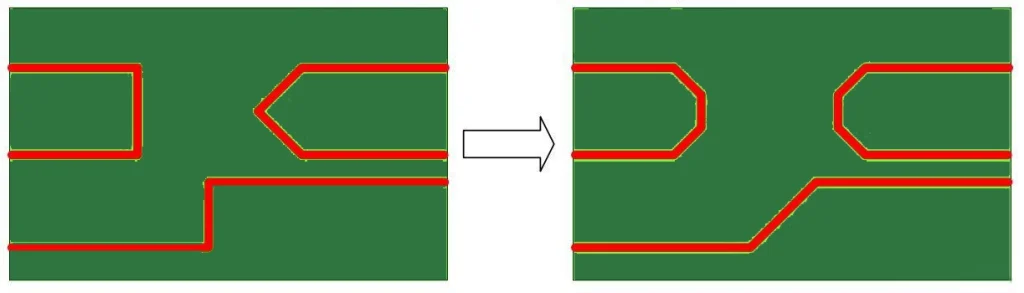
- Avoid stubs and sharp bends.


Pro Tip
Use 2D field solvers (built into Altium, KiCad) to model impedance before layout.
Mistake 5: Poor Via Design and Placement
Vias are not just holes—they’re critical interconnects.
What Happens?
- Insufficient via size: Hard to plate, leading to open circuits.
- Too few vias in power paths: High resistance, localized heating.
- Vias in pads without filling: Solder wicking, poor joint formation.
In multilayer EV PCBs, a single failed via in a ground plane can disrupt EMI shielding.
Why It’s Problematic
Designers often use default via sizes (e.g., 0.3mm drill) without considering the aspect ratio (board thickness/drill diameter). High aspect ratios (>10:1) reduce plating reliability.
DFM Fix
Follow IPC-7251 and IPC-2221B for via design. Our checklist:
- Max aspect ratio: 10:1 (e.g., 1.6mm board → min 0.16mm drill).
- For power/ground, use multiple small vias instead of one large one.
- For BGA escape, use microvias or via-in-pad with epoxy fill.
- Always specify tenting, capping, or filling in fabrication notes.


Case Example
A client used 0.2mm vias in a 2.0mm thick board (10:1 ratio). Plating voids caused intermittent failures. Switching to 0.25mm drills (8:1 ratio) resolved the issue.
Mistake 6: Copper Too Close to Board Edge
Leaving copper too close to the board edge risks edge chipping and short circuits.
What Happens?
During depaneling (V-cut or routing), copper near the edge can flake off, creating loose particles or open circuits. If power traces are affected, this can cause arcing in high-voltage systems.
IPC-2221 recommends:
- Minimum 20 mils from copper to board edge.
- 40 mils for high-voltage or high-reliability designs.
Why It’s Ignored
Designers focus on internal clearances but overlook board outline interactions.
DFM Fix
Use copper pull-back rules in your layout tool. Our checklist:
- Set a 20–40 mil keep-out zone around board edges.
- For multilayer boards, ensure internal planes also respect this margin.
- Use route keep-out layers to prevent accidental routing.
Pro Tip
For rugged applications (e.g., EV under-hood electronics), increase to 50 mils and add edge plating for EMI shielding.

Mistake 7: Inadequate Thermal Management in Layout
High-power traces must dissipate heat efficiently.
What Happens?
Without proper thermal paths, heat builds up, causing:
- Reduced component lifespan
- Solder joint fatigue
- Thermal runaway in power stages
Common Errors
- Isolated power traces with no copper pour
- Poor via stitching to the inner ground planes
- Components placed too close together
DFM Fix
Design for thermal conductivity as rigorously as for electrical performance. Our checklist:
- Use thermal relief pads for through-hole components.
- Connect power planes to traces with multiple vias.
- Add thermal vias under MOSFETs and regulators.
- Use thick copper (2–3 oz) for high-current layers.

Pro Tip
In EV inverters, use direct copper bonding (DCB) substrates or metal-core PCBs for extreme thermal loads.
Mistake 8: No Room for Testing or Assembly
Even the best design fails if it can’t be tested.
What Happakes?
- No test points for ICT or flying probe.
- Components too close for rework.
- Missing fiducials or tooling holes.
This leads to low test coverage, undetected defects, and high field failure rates.
Why It’s Missed
Designers optimize for size, not serviceability.
DFM Fix
Design for testability and repairability. Our checklist:
- Add test points for critical nets (power, ground, signals).
- Maintain 2–3 mm clearance around components for rework.
- Include global and local fiducials.
- Use 0.8–1.0 mm test pads for probe access.
Case Example
A drone ESC had no test points. Flying probe testing covered only 60%. Adding 10 test points increased coverage to 95% and reduced field returns by 40%.
Real-World Case: How DFM Saved a High-Power EV Project
A European EV startup approached us with a BMS design that kept failing during HALT (Highly Accelerated Life Testing). Initial prototypes worked, but production units showed trace burns in the 12V distribution network.

Root Cause Analysis
Our DFM review found:
- Power traces: 8 mils wide, 1 oz copper → rated for 1.5A, but peak load was 3.2A.
- Vias: Single 0.3mm via per connection → high resistance.
- Spacing: 5 mils in 60V section → risk of arcing.
Corrective Actions
- Increased trace width to 25 mils.
- Used 2 oz copper on the power layer.
- Added 3 vias per connection.
- Increased spacing to 15 mils.
Results
- The temperature rise was reduced from 45°C to 18°C.
- No failures in 1,000 units over 6 months.
- Time-to-market accelerated by 3 weeks.
This wasn’t luck—it was DFM done right.
Why Choose Our One-Stop PCB Design & Manufacturing Service?
Designing a reliable PCB isn’t just about avoiding mistakes—it’s about partnering with a manufacturer who thinks like an engineer.
Advanced Process Capabilities
- Trace/Space: Down to 3/3 mils (HDI)
- Copper Weight: 1–6 oz
- Via Types: Through, blind, buried, micro (≤0.1mm)
- Materials: FR-4, Rogers, aluminum, ceramic
- Impedance Control: ±10% tolerance
Rigorous DFM Review Process
Every design undergoes a 72-point DFM check, including:
- Trace width/spacing validation
- Current capacity analysis
- Impedance modeling
- Thermal simulation
- Testability audit
We don’t just say “your design is manufacturable”—we prove it.
Design-to-Production Integration
- Free DFM report with every quote
- Design advisory from experienced engineers
- Rapid prototyping: 5-day turnaround
- Mass production: 99.5% yield rate
Dedicated Support
Our international support team provides:
- 24/7 technical consultation and fast quoting.
- Real-time DFM feedback to prevent design errors.
- End-to-end project tracking for on-time delivery.
With our one-stop service, you can focus on innovation while we ensure your PCB designs are built right the first time.
Final Thoughts: Design Right the First Time
In the world of high-power electronics, especially in electric vehicles, there’s no second chance. A single trace design flaw can compromise safety, reliability, and brand reputation.
By avoiding these 8 critical mistakes and applying a disciplined DFM approach, you ensure your design transitions smoothly from concept to mass production.
But you don’t have to do it alone.
If you’re working on a high-reliability, high-power PCB project, send us your design files today. Our engineering team will provide a free DFM assessment and actionable feedback—no obligation.
Let’s build something that doesn’t just work, but lasts.
[Contact IWDF Solutions Team] for a free design review and fast technical consultation.