

Have you ever faced this nightmare? A critical production line grinds to a halt. A hospital’s diagnostic machine stops working. A telecom network goes dark. After frantic inspection, the culprit is discovered: a discontinued PCB with no spare parts on the market. Ordering a replacement system costs hundreds of thousands, and waiting weeks for traditional reverse engineering means crippling downtime.
Faced with this predicament, would you wait, or would you demand an immediate rescue?
At IWDF Solutions, we offer a different answer—a 48-hour PCB reverse engineering service designed for legacy equipment repair when time is your most valuable asset.
PCB reverse engineering typically takes several days or even weeks, but IWDF Solutions compresses the process into just 48 hours. Our in-house engineers scan, extract schematics, generate Gerber files, and create a replacement PCB that is 100% functionally identical to the original. This ultra-fast turnaround minimizes production downtime, saves replacement costs, and extends the life of legacy systems where no spares are available.
So how can we compress weeks of engineering into just 48 hours without cutting corners? The secret lies in our streamlined process, integrated team, and agile project management.

Seamless Collaboration: Design Team and Production Under One Roof
One of the most significant bottlenecks in traditional PCB reverse engineering is inefficient communication, which often results in prolonged project timelines. Many PCB service providers lack in-house design capabilities or dedicated production facilities, relying instead on external partners such as design houses, manufacturers, and testing laboratories—often located across different companies or even countries. Each exchange of emails, document transfer, or request for clarification introduces potential delays. Even minor misunderstandings can set a project back by several days.
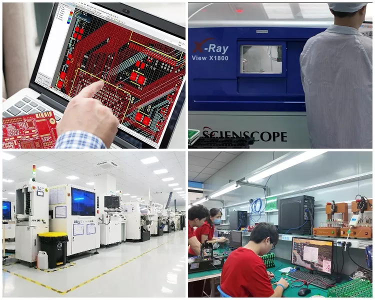
At IWDF Solutions, we eliminate that risk by keeping the entire workflow in-house:
- Zero communication delays: Our design engineers and production specialists work side by side. If there’s a question about a schematic trace or component footprint, it’s resolved in minutes, not days.
- Full process ownership: From precision scanning and image processing to schematic extraction, Gerber generation, fabrication, and electrical testing—everything is done under one roof.
- Quality assurance built into every step: We don’t just rush to finish; we run internal cross-checks to ensure the rebuilt PCB performs exactly like the original. In fact, many clients have found our boards perform better than the legacy version, as we often fix hidden design flaws during the process.
This integrated approach provides the dual guarantee of speed and quality—two factors that engineers and managers usually have to choose between.
Breaking Through Bureaucracy: Your Urgent Projects Get the Green Channel
Large OEMs and corporate repair chains often follow a rigid process:
- Submit a request.
- Wait for a sales rep.
- Wait for the project manager’s approval.
- Wait for scheduling with an external engineering team.
- Wait for production slots to open.
By the time the project begins, weeks have already been lost—and your equipment is still idle.
At IWDF Solutions, we take a different approach. For urgent reverse engineering cases, we open a dedicated green channel:
- Seamless technical liaison: Our sales specialists work in tandem with our engineering team, guaranteeing that your technical needs are translated into precise action without delay or misunderstanding.
- Instant project kickoff: As soon as we receive your PCB and requirements, work begins—no waiting for weekly planning meetings.
- Priority status: Within those 48 hours, your project becomes our sole focus. All resources are aligned toward getting your replacement PCB ready without distractions.
This agility allows us to match the urgency of your crisis—whether you’re a supply chain manager racing to restore a production line, or an R&D engineer trying to keep critical equipment alive.
Instant Feedback, Accelerated Verification Cycle
Speed doesn’t only matter in production—it matters in feedback loops. Traditional reverse engineering services often work in isolation, only delivering results at the very end. If issues are discovered late, rework and delays are inevitable.
We’ve built our process around agile iteration:
- Rapid prototyping: We can quickly produce a test version of your PCB for functional checks.
- Continuous updates: Our team provides progress reports as we scan, extract, and design, so you’re never left in the dark.
- Early validation: Potential issues are flagged and resolved before final fabrication, drastically reducing the risk of errors.
This cycle of “design → feedback → correction” ensures that even in a compressed 48-hour timeline, you get a functionally accurate PCB that works on the first try.
For engineers, that means less firefighting. For purchasing managers, it means fewer surprises. And for repair specialists, it means faster client satisfaction.
How the 48-Hour PCB Reverse Engineering Process Works
Engineers and managers often ask, “Is 48 hours really enough time?” The answer is yes—because every stage has been refined to remove delays. Here’s how we break down the process:
- Hours 0–4: Intake & Assessment
- We received your legacy PCB.
- Our engineers perform an initial evaluation.
- You receive a rapid quote and timeline confirmation.
- Hours 4–18: Scanning & Design Extraction
- High-resolution imaging captures every trace, via, and component footprint.
- We generate a rough Bill of Materials (BOM).
- Schematic extraction begins, with CAD engineers validating each net.
- Hours 18–38: Design Verification & Rapid Prototyping
- Internal review ensures schematic accuracy.
- Gerber files are generated.
- A quick-turn prototype is produced in-house.
- Hours 38–48: Testing & Delivery
- Electrical testing confirms the prototype’s functionality.
- If necessary, design optimizations are applied.
- Your verified PCB is packaged and shipped.
Note: Complex multilayer boards may require slight adjustments, but in most cases, the full process is completed in under 48 hours.
This timeline isn’t theoretical—it’s a proven workflow that has rescued clients in industries ranging from aerospace to industrial automation.
Why Is PCB Reverse Engineering the Only Option for Legacy Electronics?
When OEMs discontinue a product line, they often stop providing schematics, spares, or repair support. For companies running long-life equipment—like industrial CNC machines, MRI scanners, or defense systems—this creates a critical gap.
Reverse engineering fills that gap by:
- Reconstructing lost design data (schematics, Gerber files, BOM).
- Extending the life of expensive equipment without replacement.
- Providing a base for redesign if components become obsolete.
For procurement managers, it’s not just a technical fix—it’s obsolescence management that protects millions in capital investments.
How Long Does PCB Reverse Engineering Usually Take?
- Traditional services: Typically 2–6 weeks, especially when outsourced across multiple vendors.
- At IWDF Solutions, we combat delays or emergency projects with a priority ‘green channel’ process. Thanks to our fully in-house design and production teams, we can initiate your reverse engineering project immediately and strive for turnaround times as quick as 48 hours, getting you back online faster than our competitors.
This contrast is why our service appeals to industries where downtime costs exceed $10,000 per hour.
Is PCB Reverse Engineering Legal for Repair Purposes?
This is a common concern, especially among multinational corporations. The short answer: yes, if done for maintenance and repair.
- Allowed: Repair, replacement, or maintenance of legacy equipment when no spares or schematics exist.
- Restricted: Copying and reselling patented designs for commercial gain.
We strictly adhere to intellectual property compliance and only perform reverse engineering for clients who own or are authorized to repair the equipment.
What Deliverables Will You Receive?
Within 48 hours, clients typically receive:
- Gerber files (for fabrication)
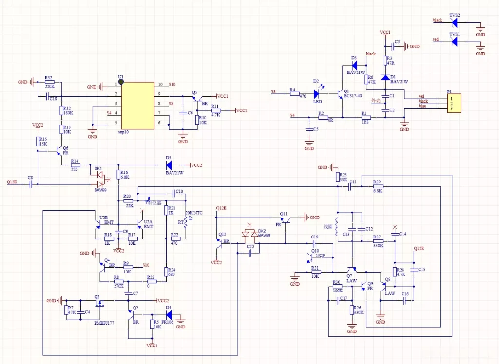
- Schematic diagrams (for documentation and future reference)
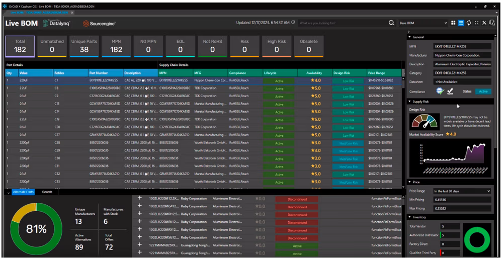
- Bill of Materials (BOM) with suggested part substitutions if original components are obsolete
- Tested replacement PCB prototype
This ensures not only an immediate fix but also future-proofing for ongoing support.


How Does Reverse Engineering Support Obsolescence Management?
For many companies, the biggest threat isn’t a single repair—it’s the long-term unavailability of parts. PCB reverse engineering plays a key role in obsolescence management strategies by:
- Creating a digital twin of legacy boards.
- Allowing redesign around available components.
- Supporting lifecycle extension for critical infrastructure.
In sectors like medical, aerospace, and industrial automation, this isn’t just cost savings—it’s regulatory compliance and operational continuity.
What to Do When Downtime Strikes
When a production line halts, or when a medical device or critical system fails, every minute matters. Waiting weeks for PCB reverse engineering isn’t an option—and replacing entire systems is rarely feasible.
That’s where IWDF Solutions steps in. With our 48-hour PCB reverse engineering service, we become your emergency response partner.
Here’s how you can take action right now:
- Call us immediately if you’re facing emergency downtime. Our technical team is available 24/7 for a quick initial assessment.
- Visit our website to learn more about our reverse engineering and obsolescence management solutions.
- Contact us for a free project estimate and quote—let’s help you get back online before losses escalate.
Final Summary
Every hour of downtime costs money. Traditional reverse engineering services take weeks, but IWDF Solutions delivers results in just 48 hours—without compromising on quality or reliability. From seamless in-house collaboration to agile prototyping, we help engineers, managers, and repair professionals rescue legacy systems when it matters most.
Don’t let downtime dictate your future—contact IWDF Solutions today and take control of legacy equipment repair.

