

Many PCB buyers are shocked by inconsistent quotes from different suppliers. Hidden design inefficiencies often drive these costs up. This article breaks down insider tips—step by step—that can help you cut PCB design and production expenses without sacrificing performance or quality.
To reduce PCB design costs, focus on minimizing the number of layers, avoiding stacked vias, selecting standard materials like FR4, and reducing board size. Efficient component selection and panelization also contribute to savings. Engage with your manufacturer early to optimize for DFM (Design for Manufacturability) and reduce unnecessary revisions.
Now, let’s explore each cost-saving tip in detail—from design to fabrication—based on real factory experience and global project insights.
How Can I Reduce the Cost of PCBs?
1. Reduce the Layer Count
In general, the more layers your PCB has, the higher your manufacturing cost. The number of layers in your PCB stackup directly affects not only material costs but also the complexity of lamination, pressing, and inspection. A 4-layer board typically costs 1.8x to 2.2x more than a 2-layer board of the same size and shape. This difference multiplies quickly in batch production.
But is a 4-layer board always necessary? Not really. Often, we’ve seen designers default to multilayer layouts to simplify routing or accommodate power planes. However, with proper component placement and trace optimization, the same layout can often be squeezed into a 2-layer design.
For example, using a solid ground pour on the bottom layer and carefully routed power traces on the top, signal integrity can be preserved even in compact IoT or wearable devices. Before increasing layers, always explore routing alternatives with your layout engineer.


2. Minimize Expensive Via Types
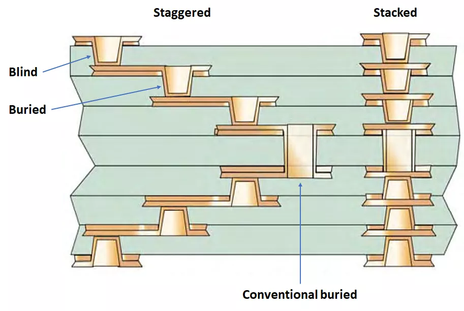
Stacked vias, via-in-pad, and microvias are useful for compact designs but drive up fabrication cost significantly. They require resin filling, copper capping, and multiple lamination cycles. Consider staggered or through-hole vias instead if space allows.
Vias are essential for connecting layers, but not all vias cost the same. Here’s a quick comparison:
| Via Type | Cost Impact | Notes |
|---|---|---|
| Through-hole | Low | Cheapest, standard across all fabs |
| Blind via | Medium | Requires sequential lamination |
| Buried via | Medium–High | More complex drilling and registration |
| Stacked via | High | Needs resin filling and capping |
If blind and buried vias are necessary, consult your manufacturer early to see how they can optimize layer-pairs for cost.
3. Stick to Standard Specifications
Use the standard 1.6mm board thickness, 1oz copper weight, standard panel sizes (18″ × 24″), and pre-approved stackups from your PCB manufacturer. Deviating from these introduces special setup steps, including different lamination profiles or unusual material preparation. Anything custom introduces complexity and tooling cost.
Ask your supplier for a “cost-optimized default stackup” before beginning the design. This alone can reduce your per-unit price by 10–15% in volume production.

How to Make PCB Cheaper During the Design Phase?
1. Involve Your Manufacturer Early (DFM Review)
Waiting until the Gerber files are complete to get feedback is a common mistake. A simple DFM (Design for Manufacturability) review can reveal costly oversights:
- Annular rings are too small for standard drill tolerances
- Trace/space widths below the fab’s standard (which incur extra cost)
- Inadequate solder mask clearances that affect the assembly
The earlier the review, the more impact it can have. Many manufacturers, including ours, offer free DFM consultations that help identify cost drivers before they lock into the layout.
2. Optimize for Panel Utilization
PCB fabs use standard panel sizes such as 18×24 inches or 16×22 inches. When your design dimensions align efficiently with these, material waste is reduced, and more boards fit per panel.
Example:
For example, a 50mm × 50mm board can fit 80–90 units per standard 18″×24″ panel. But increasing the board to 53mm × 53mm may reduce the number to around 70, raising per-unit cost by up to 20%.
That small 3mm increase can lead to a 30–40% increase in per-unit fabrication cost. Always confirm panel utilization before finalizing your board outline.
3. Combine Designs to Share Setup Costs
If you’re running multiple small boards or prototypes, you can combine them into a single panel using step-and-repeat formatting.
This way, you only pay one set of setup charges (tooling, stencil, etc.) rather than per board.
What Is the 3W Rule in PCB Design and Why Does It Matter?
The 3W rule states that the distance between two signal traces should be three times the width of the trace. For example, if your trace width is 6 mil, the gap between adjacent traces should be at least 18 mil.
This spacing reduces electromagnetic coupling (crosstalk) between traces. Why is this important for cost?
- Crosstalk causes signal integrity issues that can fail EMC/EMI compliance tests
- Boards that fail testing must be redesigned and retested, increasing time-to-market and cost
- Using adequate spacing also allows for standard fab tolerances, avoiding the need for microfabrication
By following the 3W rule and maintaining clearances per IPC guidelines, you prevent costly production failures.

How Much Does PCB Design Typically Cost? Can You Save Here?
Outsourcing PCB design can become expensive fast. Based on our industry experience, here’s a breakdown of common costs:
| Task | Time Estimate | Rate (USD/hour) | Total Cost |
|---|---|---|---|
| Schematic Design | 30–50 hrs | \$80–\$120 | \$2,400–\$6,000 |
| Layout Design | 40–60 hrs | \$100–\$150 | \$4,000–\$9,000 |
| Routing Optimization | 20–40 hrs | \$90–\$130 | \$1,800–\$5,200 |
How to Save on Design:
- Use reference designs from chip vendors
- Choose components with open-source footprints available
- Avoid frequent layout revisions—each change adds hours
Design costs are easiest to control when the scope is clear from the start. Always define the signal speed, mechanical outline, and component list upfront.
What Materials and Finishes Help Reduce PCB Fabrication Cost?
1. Base Material: FR4
FR4 is a glass-reinforced epoxy laminate that supports most digital, analog, and low-RF applications. It’s cost-effective and globally available.
Here’s a cost comparison:
| Material | Relative Cost | Applications |
|---|---|---|
| FR4 | Low | Standard |
| High-Tg FR4 | Medium | High temp, automotive |
| Rogers | High | RF, Microwave |
| Polyimide | High | Flex/rigid-flex |
Only use high-frequency materials (Rogers, PTFE) if required by your application specs.
2. Finish Selection: Avoid Over-Specifying
Surface finish affects solderability and shelf life. ENIG is common, but not always needed.
| Finish | Cost Impact | Use Case |
|---|---|---|
| HASL | Low | Through-hole, general use |
| OSP | Low | Fine-pitch SMT |
| ENIG | High | BGA, fine pitch, long shelf-life |
Ask your assembler what’s sufficient—often OSP is enough, saving up to 20% on finishing costs.
What Are Cost-Effective PCB Layout Practices?
1. Minimize PCB Size
Material costs are panel-based. Shrinking board dimensions allows more units per panel, thus reducing the cost per piece. However, make sure spacing is not compromised—overcrowded layouts cause solder bridges and test failures.
2. Use Common Shapes
Avoid complex contours, inner cutouts, and irregular outlines. These require special CNC routing and increase the likelihood of breakage during depaneling.
Stick to rectangles or squares when possible—they maximize yield and minimize machining cost.
3. Standardize Drill Sizes
Use only a few standard hole diameters (e.g., 0.3mm, 0.6mm, 0.8mm). Each additional size requires a tool change, which slows down production and adds setup time.
Reducing drill size count from 8 to 3 can lower drill costs by up to 15% in batch runs.
How to Reduce PCB Assembly Cost?
Assembly cost is driven by machine setup, part sourcing, and inspection.
1. Pick Standard Packages
Choose parts in standard SMT packages: 0603, 0805, SOT-23, QFP, etc. Avoid legacy packages (PLCC), large through-hole parts, or extremely fine-pitch BGAs unless necessary.
Using exotic or oversized parts means:
- Higher pick-and-place setup cost
- Lower machine speed
- More manual inspection is required
2. Prefer One-Side Placement
Double-sided boards require double the reflow passes and stencils. This increases thermal stress and labor cost.
Try to place all components on one side—especially for prototypes and small runs. If two-sided is unavoidable, place low-heat parts on the bottom.
3. Add Clear Silkscreen
A well-labeled silkscreen improves manual inspection and testing efficiency. This reduces human errors and speeds up quality control.
Which PCB Fabrication Tips Can Cut Down Production Waste?
1. Align with Panel Standards
Ask your fab what their standard panel size is and design your boards to nest efficiently within that frame.
If your board is just a few mm too wide, it may force the fab to drop one unit per panel, increasing cost by 15–20%.
2. Minimize Routing Complexity
Avoid long internal slots, curves, or tiny radius corners unless necessary. These features slow down the CNC machines and increase reject rates.
Keep the outline simple and define breakaway tabs clearly if you’re using V-cut or mouse-bites for depaneling.
Summary
Cost-effective PCB design is not just about cheap materials—it’s about smart decisions. Follow these tips, consult your manufacturer early, and you’ll cut costs significantly while boosting reliability. Got questions or want help reviewing your current design? Let’s talk.
FAQs
Q1. Does bulk ordering PCBs really save money?
Yes, bulk orders reduce setup costs (tooling, stencils, programming) since these are shared across more units. Volume pricing also drives down the per-unit cost.
Q2. Is there a big cost difference between quick-turn PCBs and standard lead time?
Absolutely. Quick-turn services add a premium (sometimes +30–50%) because they require overtime scheduling and priority in production. Planning early and using standard lead times is a simple way to save.
Q3. Do PCB shape and outline complexity affect manufacturing costs?
Yes. Odd shapes, internal cutouts, or curves require extra CNC routing, which takes longer and increases panel waste. Simple rectangular outlines are cheaper to fabricate.
Q4. Can reducing the number of unique drill sizes lower PCB cost?
Yes. Each additional drill size means a tool change and extra machine calibration. Standardizing hole sizes keeps drilling faster and lowers production cost.
Q5. Are flexible PCBs always more expensive than rigid PCBs?
Generally, yes. Flex and rigid-flex PCBs require specialized materials (polyimide films), more complex lamination, and careful handling. Unless necessary, rigid PCBs are more cost-effective.
Q6. What’s the cheapest PCB surface finish for prototypes?
HASL (Hot Air Solder Leveling) is usually the most economical. OSP is also inexpensive for fine-pitch SMT. ENIG and other high-end finishes should only be chosen if your design requires them.
Q7. Does using smaller trace/space rules always increase PCB cost?
Yes. The tighter the design rules (e.g., <4 mil traces/space), the more advanced fabrication processes are needed. Sticking to your manufacturer’s standard capabilities avoids premium charges.

