
Flex PCB Design That Bends Without Limits
Engineer Lighter, Denser, and More Reliable Electronics with Custom Flex PCB Solutions

Why Choose Flex PCB Design?
Flex PCB design unlocks product possibilities once limited by space, weight, or movement—empowering engineers to create lighter, more durable devices that thrive where rigid boards cannot. It’s not just about bending circuits; it’s about rethinking design boundaries to build compact, ergonomic, and reliably adaptive solutions for today’s dynamic applications.

Space Efficiency
Optimize every millimeter of your device with ultra-thin, bendable layouts that reduce weight and size.

High Reliability Under Stress
Flex circuits withstand vibration, thermal cycling, and mechanical movement far better than rigid boards.

Streamlined Assembly
Reduce connectors, cables, and assembly complexity—boosting both reliability and manufacturing efficiency.
Our Flex PCB Design Capabilities
Our engineers collaborate closely with clients to ensure each flex PCB design is optimized for functionality, manufacturability, and long-term reliability. Whether you need a single-sided flex or a complex rigid-flex structure, we design with your real-world applications in mind.
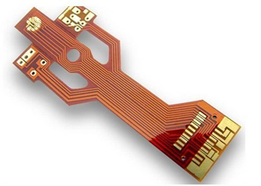
Single-sided, double-sided, and multilayer flex PCB design
Rigid-flex PCB integration
Controlled impedance and high-speed signal routing
Tight bending radius optimization
3D mechanical fit verification
EMI/EMC design considerations
Material selection (PI, PET, adhesiveless laminates)
Stack-up design and cost-performance balancing
Supporting Subheading
A Transparent Process from Concept to Production
A successful flex PCB isn’t just designed on a screen—it’s meticulously engineered through a collaborative, detail-oriented process. We partner with you at every step to transform your concept into a high-reliability, production-ready product, proactively addressing electrical, mechanical, and manufacturability challenges before they become costly delays.
Requirement Analysis
We begin by thoroughly documenting your product's functional needs, operational environment, and lifecycle goals. This goes beyond circuit schematics to include critical mechanical constraints like bend cycles (static vs. dynamic), fold angles, installation space, and environmental exposures to heat, moisture, and chemicals。
Schematic Capture & Initial Layout Planning
Our engineers create the circuit schematic, defining the electrical connectivity. Simultaneously, we plan the initial board outline and critical component placement in 3D space, considering how the flex circuit will bend and fit within your assembly. This early spatial planning is crucial for avoiding assembly issues later.
3D Mechanical Modeling & FEA Simulation
We integrate our PCB layout into your product's mechanical CAD model. Using Finite Element Analysis (FEA), we simulate stress, strain, and fatigue at proposed bend areas, identifying potential failure points and optimizing the flex circuit geometry and copper routing before prototyping.
Stack-Up Engineering & Material Selection Advisory
This is where flex design expertise truly shines. We advise on the optimal layer stack-up and recommend specific materials—such as polyimide thickness, copper type (RA/ED), and adhesive systems—to achieve the perfect balance of flexibility, thermal performance, and signal integrity for your application and budget.
DFM-Optimized Routing & Critical Rule Definition
Our layout engineers route the board with a strict set of flex-specific design rules. This includes managing copper strain relief, avoiding acute angles, defining neutral bend axes, and keeping vias away from high-stress areas to ensure long-term reliability and high manufacturing yield.
Prototyping, Design Validation & Rapid Iteration
We fabricate functional prototypes and put them through rigorous testing—from basic electrical continuity to dynamic flex endurance and environmental stress testing. This phase validates our design assumptions and allows for rapid iterations, de-risking your final product.
Flex PCB Manufacturing Process & Workshop
A flawless design deserves an equally precise manufacturing execution. In our state-of-the-art, climate-controlled facility, your flex PCB designs are transformed into reality through a rigorous process tailored for the unique demands of flexible materials. We maintain strict process control to ensure every circuit we ship meets the highest standards of reliability and performance.
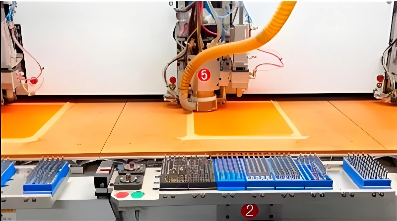
Precision Material Preparation & Laser Drilling
We start with high-quality polyimide or PET substrates, utilizing laser drilling to create microvias with exceptional accuracy and clean walls, which is critical for fine-line flex and HDI designs.
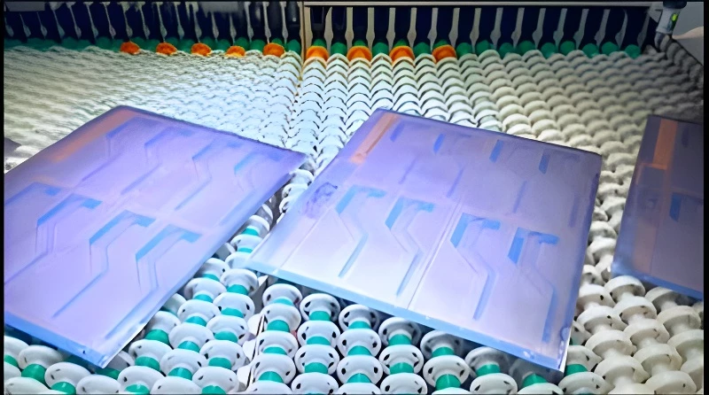
Advanced Pattern Imaging & PLC Control
Using laser direct imaging (LDI) technology, we transfer your circuit pattern with ultra-fine resolution. Every panel is tracked by our Programmable Logic Controller (PLC) system, ensuring traceability and preventing mixed batches.

Electroplating & Panel Plating
We build a reliable electrical connection through panel plating, ensuring uniform copper deposition in through-holes and vias. This step is vital for the conductivity and durability of your flex circuits, especially in dynamic flex applications.
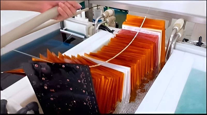
Coverlay Lamination & Precision Surface Finish
Instead of a standard solder mask, we use a flexible coverlay for superior protection and flexibility. We then apply the optimal surface finish (such as ENIG or Immersion Silver) to ensure a solderable, flat, and reliable surface for your components.
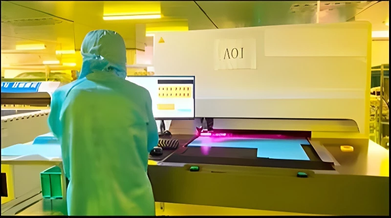
Advanced Pattern Imaging & PLC Control
100% of boards undergo flying probe electrical testing to verify netlist connectivity. Automated Optical Inspection (AOI) meticulously scans each layer, catching any subtle defects in traces or soldermask to ensure integrity.
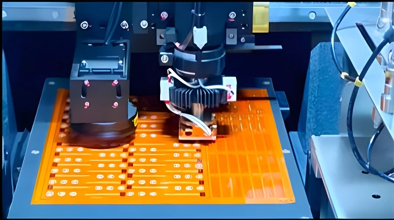
Final Profiling & Singulation
Using highly accurate laser cutting or precision die-cutting, we outline the final flexible shape from the production panel. This method delivers clean, burr-free edges without mechanical stress, which is crucial for the delicate structures of flex circuits.
IWDF Solutions PCB's Flexible PCB Manufacturing Capability
Transparency builds trust. Here are the key technical specifications of our flex PCB manufacturing capabilities, empowering you to make an informed decision with the confidence that we can deliver to your exact requirements.
| Capability Item | Our Specifications |
|---|---|
| Max Layer Count | 1-12 Layers (Flex & Rigid-Flex) |
| Base Material | Polyimide, PET, PTFE |
| Min. Trace/Space | 2/2 mil (0.05mm / 0.05mm) |
| Min. Laser Drill Size | 0.1mm (4 mil) |
| Board Thickness | 0.05mm - 0.5mm |
| Max. Panel Size | 24" x 24" |
| Surface Finish | ENIG, ENEPIG, Immersion Silver, OSP, Hard Gold |
| Coverlay | Polyimide, PSA (Pressure Sensitive Adhesive) |
| Control Impedance | ±10% tolerance |
| Certifications | ISO 9001, IATF 16949, UL Certified |
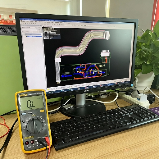
Why Choose Us for Flex PCB Design?
We don’t just design boards—we design solutions that flex, fold, and fit where others can’t. With deep expertise in both electrical performance and mechanical integration, we help you avoid common flex circuit pitfalls and achieve a faster path to market.
- Flex-Specific Experience – Over [X] years designing flex and rigid-flex PCBs for demanding applications.
- Seamless Design-to-Production – As your one-stop PCB partner, we ensure your design is both innovative and manufacturable.
- Collaborative & Responsive Support – You work directly with engineers who understand both circuit design and real-world assembly.
Powering Innovation Across Industries
Flex PCBs are the backbone of modern electronics, enabling breakthroughs where standard rigid boards fall short. From life-saving medical equipment to next-generation automotive systems, our flex design expertise helps innovators conquer the challenges of space, weight, and dynamic movement. Explore the industries we serve:
Diagnostic Imaging: Portable ultrasound probes, endoscopic capsules.
Patient Monitoring: Wearable patches, continuous glucose monitors.
Implantable Devices: Pacemakers, neurostimulators, hearing implants.
Surgical Tools: Robotic surgery arms, disposable surgical instruments.
ADAS & Sensors: LiDAR, radar, camera modules.
In-Cabin Systems: Curved display backplanes, seat control units, ambient lighting.
Powertrain & Battery Management: Battery monitoring systems (BMS), inverter controls.
Vehicle Connectivity: GPS modules, infotainment systems.
Avionics: Cockpit displays, flight control systems.
Satellite Systems: Deployable solar panels, satellite communication.
UAVs & Drones: Gimbal controls, lightweight flight controllers.
Military Equipment: Wearable soldier systems, ruggedized communication devices.
Mobile Devices: Smartphone foldable displays, compact camera modules.
Computing: Laptop hinge connectors, wearable tech.
Audio: Wireless earbuds, neckband headphones.
Gaming & VR: VR headset headbands, console controllers.
Industrial Robotics: Robotic arm joints, sensor arrays.
Condition Monitoring: Wireless vibration sensors, predictive maintenance tags.
Smart Agriculture: Equipment telematics, environmental sensors.
Factory Automation: PLCs, motor drives, HMI panels.
5G Infrastructure: Active Antenna Units (AAUs), small cell radios.
Optical Networking: High-speed transceivers, router interconnects.
Server & Storage: High-density server interconnects.
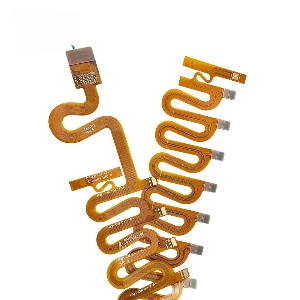
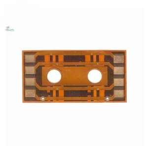
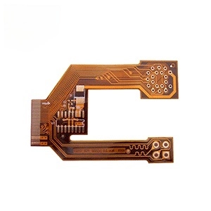
Case Display
From Prototypes to Production-Ready Boards
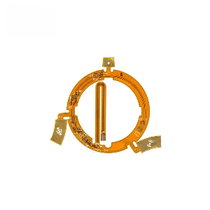
Ready to Design a Flex PCB That Moves With Your Vision?
It depends on layer count and materials, but we typically design for 6-10x the flex thickness for dynamic applications—and guide you through every step.
Yes. We design for both bare flex and assembled flex circuits, accounting for mechanical stress and thermal expansion
Through careful material selection, copper plating options, and avoiding vias in bend zones—backed by simulation and testing.
Initially, yes—but they often reduce total cost by eliminating connectors, cables, and assembly steps.