

What Is a Gerber File in PCB Design?
A Gerber file is a 2D vector image file that describes the shapes and positions of each PCB layer (copper, solder mask, silkscreen, etc.) so that a manufacturer can fabricate your board exactly as designed. Each PCB layer is typically exported as a separate Gerber file, along with drill data and a clear board outline. Together, these files act as the blueprint of your PCB for the fabrication and assembly process.

Why Gerber Files Matter for Reliable PCB Manufacturing
From PCB Layout to Fabrication Machines
Your PCB layout tool shows traces, pads, planes, and graphics on screen, but fabrication equipment cannot read your design database directly. Gerber files convert this layout into standardized 2D layer images that photoplotters, imaging machines, and CAM software can understand.
For each layer, the Gerber file encodes the exact geometry and location of copper tracks, pads, solder mask openings, silkscreen legends, and other features. When combined with NC drill files and stack‑up information, manufacturers can drive processes such as photoimaging, drilling, plating, solder mask coating, and routing with high precision.
Typical Problems When Gerber Data Is Wrong
When Gerber data is incomplete or inconsistent, even a good factory cannot guess your intent. Typical issues include:
- Misaligned or missing board outline, leading to incorrect board size or shape.
- Drill files that do not match pad positions, causing off‑center holes or broken annular rings.
- Wrong units or coordinate precision, which can scale or shift the entire design.
- Solder mask not aligned with pads, creating shorts or insufficient solderable areas.
- Silkscreen printed on pads, interfering with soldering and inspection.
These problems can cause scrap, delays, or forced redesigns, especially when working with overseas suppliers, where each iteration costs extra time.
Main Types of Gerber‑Related Files You Must Provide
Copper Layer Gerbers (Signal and Plane Layers)
Copper layer Gerbers define all conductors on your board: traces, pads, copper pours, and planes. For a 2-layer board, you will have top and bottom copper layers, while a 4-layer board typically includes two inner layers for signals or power/ground.
Common issues include missing thermal reliefs on planes, excessively small trace/space relative to the manufacturer’s capability, or copper features too close to the board edge. It helps to confirm the factory’s minimum trace/space and annular ring capabilities and ensure your design rules match these before generating Gerbers.
Solder Mask Layers
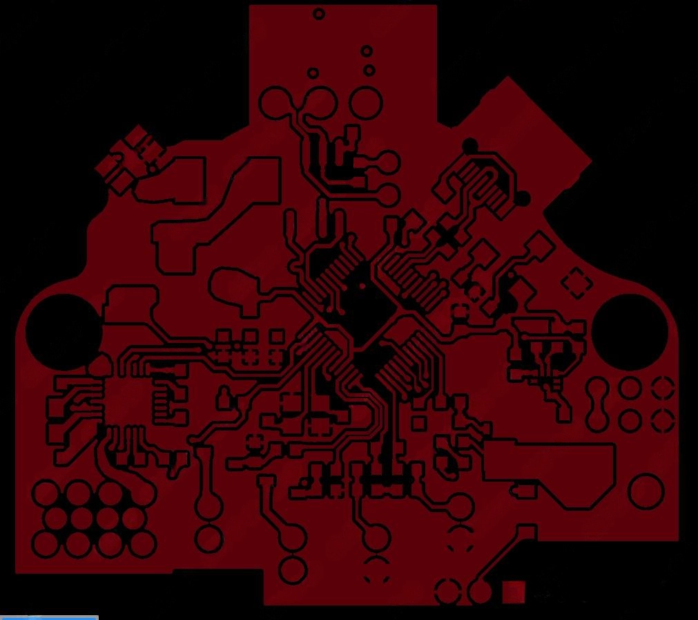
Solder mask Gerbers define which areas of the board will be covered with protective lacquer and which areas will be left exposed for soldering. Pads and selected openings are kept clear, while the rest of the surface is covered to prevent solder bridges and corrosion.
Good solder mask design practices include:
- Checking that the mask is not accidentally inverted (copper covered, non‑copper exposed).
- Keeping a reasonable mask expansion around each pad to ensure reliable soldering.
- Avoid extremely narrow mask dams that your fabricator cannot hold.

Silkscreen Layers
Silkscreen layers contain reference designators, component outlines, polarity marks, and other text that help during assembly, testing, and field repair. Poorly designed silkscreen can confuse or interfere with soldering if it overlaps pads.
Design guidelines you can follow:
- Keep the silkscreen at least a small clearance away from pads and exposed copper.
- Use line widths and text heights that meet or exceed your fabricator’s minimum recommendations.
- Avoid putting critical polarity or orientation marks only on the top side if components or assembly operations are present on both sides of the PCB.
Drill Files (NC Drill and Drill Map)
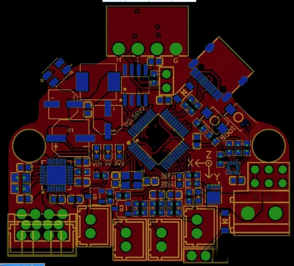
Drill files (often Excel format with .DRL extension) Specify the positions and sizes of all holes in your PCB, both plated and non‑plated. Some tools generate separate files for plated and non-plated holes, which can help clarify the stack-up and mechanical features.
A good drill file set should include:
- The main NC drill file with coordinates and tool sizes.
- A drill rack or tool list (sometimes embedded in the header).
- Optional drill map in Gerber format, visually showing hole sizes and locations.
Errors such as mismatched units, missing tool definitions, or misaligned origins can cause severe manufacturing issues, so this is a critical area to verify.

Board Outline / Mechanical Layer
Your board outline defines the final cut shape of the PCB, including slots and internal cutouts. Some tools generate a dedicated mechanical or outline layer (e.g., .GKO) that the factory uses to program routing or V‑cut paths.
To avoid confusion, make sure that:
- There is one clear, closed outline on a dedicated layer.
- Dimension lines or other markings are not drawn with the same line style as the outline.
- Any special mechanical details like chamfers or break‑off tabs are clearly indicated.
Assembly Drawing and Pick‑and‑Place (for PCBA)
Although not Gerber files in the strict sense, assembly drawings and pick‑and‑place files are often delivered alongside Gerbers for PCBA orders. Assembly drawings show component outlines, reference designators, and polarity marks on each side of the board, while pick‑and‑place files give precise component coordinates and rotations for SMT machines.
Providing clear assembly data reduces the risk of mis‑placed components, especially when working with an overseas partner that cannot ask quick questions on site.

Gerber File Formats
The Gerber standard has evolved over decades. Understanding the differences helps engineers choose the right export settings.
RS-274D (Obsolete)
RS‑274D is the original “standard Gerber” format that was created in the era of numerical‑control photoplotters. It provides basic plotting instructions (moves, draws, flashes) but does not include aperture definitions or configuration inside the file itself. Instead, designers had to send separate aperture tables describing pad and trace shapes, which made jobs easy to misinterpret if those tables were missing or out of date. Because of this extra dependency and the limited way graphics are described, RS‑274D is now considered a legacy format and is only kept for very old designs. For any new PCB project, you should avoid RS‑274D output and switch to a modern format.
- Introduced in the 1960s.
- Required an extra file called an “aperture list” to define shapes.
- Error-prone because missing aperture lists made files unreadable.
- Rarely used today.
RS-274X (Extended Gerber)
RS‑274X, often called “Extended Gerber,” is today’s mainstream production format. It uses human‑readable ASCII commands to describe a 2D image of each PCB layer and, more importantly, bundles all key details into one self‑contained file. A typical RS‑274X layer file includes configuration parameters, units and coordinate format, aperture definitions, and the XY draw/flash commands for the actual geometry. This eliminates the need for separate aperture tables and greatly reduces ambiguity. Most EDA tools generate RS‑274X by default, and most PCB manufacturers expect this format when they ask for “Gerber files,” even if extensions like .gbr, .gtl, or .gbl differ between tools.
- Introduced in the 1990s, and quickly became the industry standard.
- Self-contained: no need for separate aperture files.
- Supports polygons, complex shapes, and embedded attributes.
- Still widely used and accepted by nearly all manufacturers.
Gerber X2 (Latest)
Gerber X2 is an extension of RS‑274X that keeps the same graphics language but adds attributes to describe what the data actually represents. With X2, you can tag each file and even individual features with functions such as “top copper,” “bottom solder mask,” “via pad,” or “fiducial,” instead of relying only on file names and layer order. These attributes make automated CAM import, rule checking, and documentation more reliable, because the manufacturer no longer needs to guess layer roles from naming conventions. Many modern CAD tools already support exporting Gerber X2, and more advanced PCB factories can use this extra information to streamline their front‑end process. If your tool and supplier both support it, choosing X2 for new designs gives you clearer, more future‑proof manufacturing data while staying backward‑compatible with RS‑274X viewers.
- Released in 2014 by Ucamco (the custodians of the Gerber format).
- Adds layer-specific attributes such as:
- Pad functions (SMD pad, via, test pad)
- Net names
- Layer intent (solder mask, silkscreen, copper)
- Improves automation by giving factories more context.
Today, RS-274X and X2 are the dominant formats. Unless your manufacturer specifies otherwise, exporting in RS-274X is the safest choice.
Gerber File Contents and Their Functions
| File / Layer Name | Common File Extension | Purpose / Description |
|---|---|---|
| Top Copper Layer | .GTL | Defines copper traces, pads, and planes on the top side of the PCB. |
| Bottom Copper Layer | .GBL | Defines copper routing and ground/power planes on the bottom side. |
| Top Solder Mask | .GTS | Shows areas where solder mask is not applied, exposing pads for soldering. |
| Bottom Solder Mask | .GBS | Same as the top mask, but for the bottom layer of the PCB. |
| Top Silkscreen | .GTO | Displays component outlines, labels, and logos on the top side. |
| Bottom Silkscreen | .GBO | Displays text and markings on the bottom side for identification or orientation. |
| Board Outline / Mechanical Layer | .GKO / .GML | Defines the exact board shape, dimensions, and mechanical cutouts or slots. |
| Drill File (NC Drill) | .TXT / .DRL | Specifies all drilled hole locations, diameters, and tool data for vias and components. |
| Solder Paste Layers | .GTP / .GBP | Used for stencil manufacturing; defines where solder paste is applied during assembly. |
| Fiducial / Tooling Layer | .GTL / Custom | Contains alignment marks and mechanical holes used by automated pick-and-place machines. |
| Copper Pour / Plane Layer | Included in .GTL / .GBL | Represents large filled copper areas for power or ground connections, improving current flow and EMI performance. |
| Panelization Information | .GTPNL / Custom | Defines how multiple boards are arranged together on one panel for efficient production. |
How to Generate Gerber Files from Common PCB Design Tools
General Workflow (Most EDA Tools)
Most modern PCB design tools follow a similar high‑level process for creating Gerbers:
- Complete your schematic and PCB layout, meeting your design rules.
- Configure your layer stack‑up and confirm copper thickness and board thickness.
- Open the CAM or fabrication output dialog (e.g., “Plot,” “CAM Processor,” or “Generate Fabrication Files”).
- Select output format as Gerber RS‑274X and enable each required layer (copper, mask, silkscreen, outline, paste, etc.).
- Generate NC drill files with matching units and coordinate format settings.
- Export all files into a single project folder or compressed ZIP.
- Open the resulting files in an independent Gerber viewer and verify every layer and drill hole.
Even if your EDA tool has “one‑click order” integration with a specific manufacturer, following these steps helps you understand what is actually being sent and ensures that you can work with any PCB factory in China or elsewhere.
Altium Designer: Exporting Gerber and NC Drill
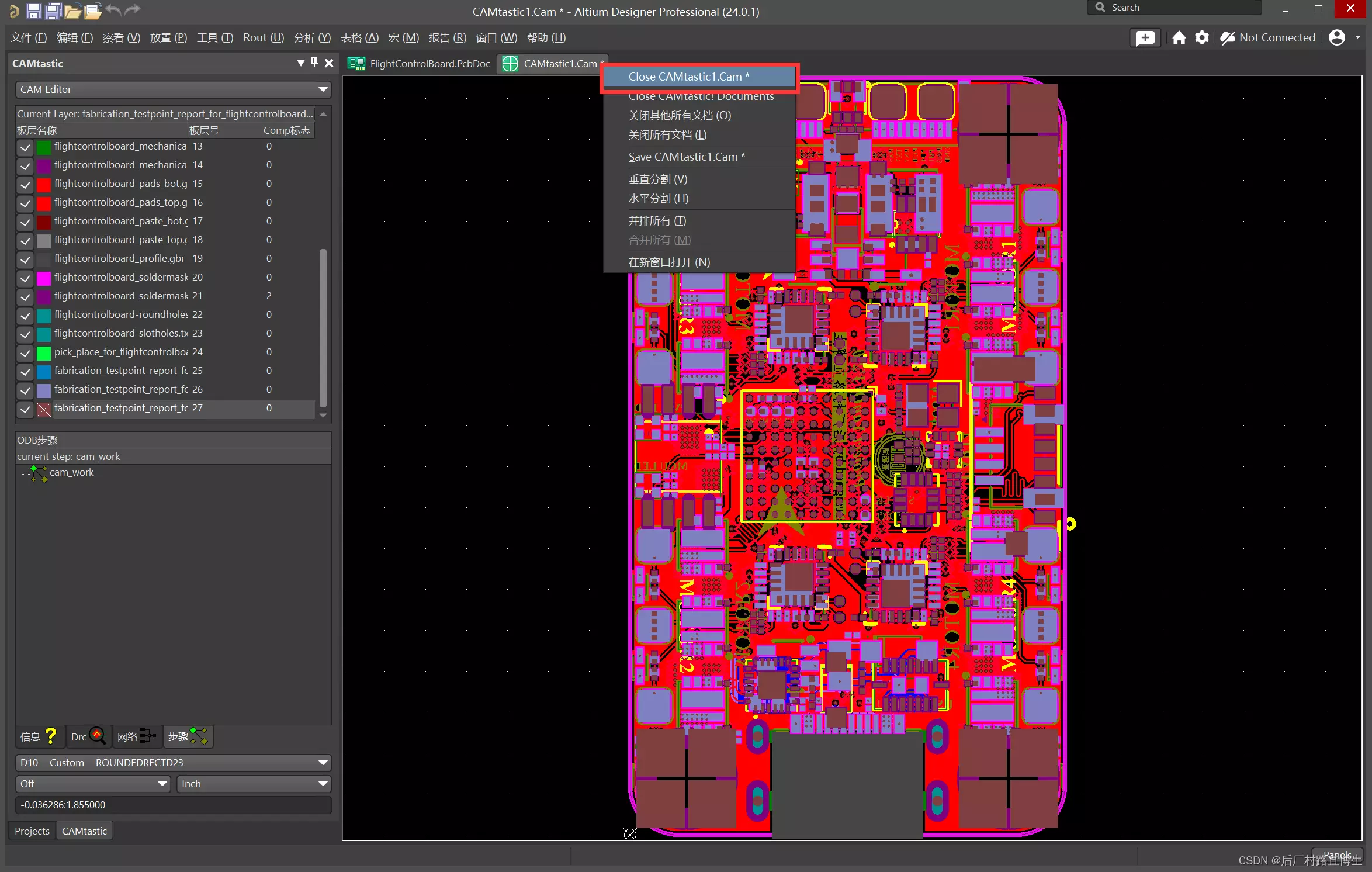
In Altium Designer, you typically use the CAM output or file fabrication outputs to generate Gerbers and NC drill files. The main practical points are:
- Use RS‑274X and absolute coordinates.
- Ensure that all fabrication layers you need are enabled.
- Generate drill files with the same origin and units as your Gerbers.
Altium also lets you define layer pairs and specific fabrication notes, which you can include in a mechanical or notes layer for your manufacturer.
KiCad: Generating RS‑274X Gerbers
KiCad provides a straightforward “Plot” dialog for Gerber output. The common practice is:
- Choose “Gerber” as the plot format and select the required layers.
- Enable “Use Protel filename extensions” if your manufacturer prefers that convention.
- Export drill files with the “Generate Drill Files” dialog, matching units and format.
After plotting, KiCad users usually inspect the package in a separate Gerber viewer or a viewer integrated with the fabrication service they plan to use.
Eagle and Other EDA Tools: Key Settings to Check
Other tools, such as Eagle, OrCAD, or EasyEDA have similar dialogs to generate Gerber and drill files. Whatever tool you use, the essential checks remain:
- Confirm RS‑274X format, not the legacy RS‑274D.
- Make sure the same origin and units are used for all layers and drill files.
- Verify that each layer is correctly mapped (top copper as top layer, not silkscreen, etc.).
Many tools and manufacturers provide detailed step‑by‑step instructions for specific combinations (e.g., EasyEDA → JLCPCB), which you can follow as a starting point.
Checklist: What a Manufacturer‑Ready Gerber Package Should Contain
Before you send files to a PCB factory in China or elsewhere, you should be able to tick off a clear checklist. The table below summarizes what a complete, manufacturer‑ready package usually includes.
| Item | Required? | Practical Notes for PCB Manufacturers in China |
|---|---|---|
| Top/Bottom copper Gerbers | Yes | Make sure track widths and clearances match the factory’s minimum capabilities. |
| Inner layer Gerbers (if multilayer) | If multilayer | Layer order should match the documented stack‑up from top to bottom. |
| Solder mask layers (top/bottom) | Yes | Check openings around pads; confirm mask is not accidentally inverted. |
| Silkscreen layers (top/bottom) | Optional but recommended | Avoid text on pads; use manufacturable line widths and text size. |
| Board outline / mechanical layer | Yes | Use a single closed outline; avoid extra overlapping contours. |
| NC drill files (PTH/NPTH) | Yes | Units and origin must match the Gerber files; include tool list if possible. |
| Paste mask layers (for stencil) | If SMT stencil is needed | Some factories generate these from pads, but explicit files give you more control. |
| Assembly drawings | Strongly recommended | Clarify component outlines, reference designators, and polarity marks. |
| Readme/notes (text or drawing layer) | Strongly recommended | State material, thickness, copper weight, finish, color, special instructions. |
Many manufacturers publish similar checklists, all emphasizing the same core idea: clear, consistent files significantly reduce questions and risk.
Common Gerber File Mistakes and How to Avoid Them
Even experienced engineers make avoidable mistakes when preparing Gerber files. Below are some of the most frequent problems and practical ways to prevent them.
1. Missing or Ambiguous Board Outline
If the board outline is drawn on multiple layers, or not clearly closed, the CAM engineer may have to guess where to cut, which can lead to wrong board dimensions.
Avoid this by:
- Using a dedicated outline/mechanical layer.
- Ensuring a single, continuous contour defines the outer edge.
- Labeling internal cutouts or keep‑out areas clearly.
2. Incorrect Units or Coordinate Format
When drill files use inches and Gerbers use millimeters, or when coordinate formats differ, drill holes can appear in the wrong locations in CAM tools.
Prevent this by:
- Selecting a single unit system (usually millimeters) for all outputs.
- Confirming coordinate format (for example, 3:3 or 4:2) is consistent across layers.
- Checking alignment in an external Gerber viewer before sending files.
3. Drill Files Not Matching Pads
If the drill file origin does not match the Gerber origin, or if pad sizes do not match drill sizes, you can end up with off‑center holes or broken annular rings.
You can mitigate this by:
- Using the PCB origin as the common reference for both copper and drill.
- Reviewing one layer at a time in a viewer with copper and drills enabled to confirm alignment.
- Ensuring drilled holes are within the manufacturer’s minimum annular ring capability.
4. Silkscreen on Pads
Silkscreen lines or text that overlap pads can be scrubbed off during soldering or create contamination, leading to unreliable joints.
To avoid this:
- Set silkscreen‑to‑pad clearance rules in your design tool.
- Run DRC checks that flag silkscreen violations.
- In your text, leave enough clearance around fine‑pitch components like QFNs or BGAs.
5. Solder Mask Misconfiguration
Incorrect solder mask openings can cause shorts (mask too open) or insufficient solder wetting (mask too restricted).
Good practice includes:
- Reviewing padstack definitions for mask expansion.
- Checking solder mask layers in a viewer to confirm openings around pads are correct.
- Avoiding extremely narrow mask dams that exceed the minimums your manufacturer specifies.
6. No Clear Distinction Between Plated and Non‑Plated Holes
If your design includes mounting holes or slots that should not be plated, but these are not differentiated, the factory may treat everything as plated.
To clarify:
- Use separate drill files or tool codes for plated and non‑plated holes where possible.
- Indicate NPTH in your drill notes or fabrication drawing.
7. Skipping Independent Gerber View Verification
Many issues are only obvious when you see how all layers stack together, yet some designers ship files without a final visual check.
Make it a habit to:
- Always load the complete Gerber package into an independent viewer (such as Gerbv or the viewer your manufacturer recommends).
- Inspect copper, mask, silkscreen, drills, and outline for every new project before sending.
Taking 10–15 minutes to check can save days of email back‑and‑forth, especially across time zones.
How Gerber Files Fit into the End‑to‑End PCB & PCBA Workflow
From Schematic to Gerber to Assembly
Gerber files sit in the middle of the full hardware development flow. A typical path looks like this:
- Capture schematic, define components, and verify the circuit.
- Design PCB layout, routing signals and arranging layers.
- Generate Gerber and NC drill files that describe each layer and hole.
- Fabricate bare PCBs using those files: imaging, etching, drilling, plating, solder mask, legend, and profiling.
- Use BOM, pick‑and‑place files, and assembly drawings to mount components on the fabricated boards (PCBA).
Gerber files bridge design and manufacturing: if they are accurate and well structured, the entire downstream process becomes more predictable.
What Your PCB Factory in China Actually Does with Your Gerber Files
When a factory receives your Gerber package, CAM engineers import each layer into specialized software. They check layer alignment, generate phototools for imaging copper and solder mask, plan drill programs, and define rout paths for profiling.
They also apply process‑specific rules, such as adding test points, optimizing clearances for manufacturability, and sometimes adjusting paste apertures for better soldering performance. If anything in your files is unclear, they need to stop and ask questions, which adds time and risk—especially across language and time‑zone barriers.
Providing clean, well‑documented Gerber files allows your factory partner to focus on process optimization rather than file repair.
What Your PCB Supplier Needs Besides Gerber Files
Gerber files themselves describe geometry, but they do not fully specify materials, finishes, or acceptance criteria. For a smooth project, you should also share:
- Layer stack‑up and material requirements: number of layers, core/prepreg scheme, FR‑4 or other materials, and any impedance‑controlled layers.
- Board thickness and copper weight: for example, 1.6 mm board with 1 oz copper on all layers.
- Surface finish: HASL, lead‑free HASL, ENIG, immersion silver, or others, depending on your reliability and cost needs.
- Solder mask and silkscreen colors: typical combinations are green mask with white silkscreen, but many factories support multiple colors.
- Special via types: such as blind/buried vias, via‑in‑pad, or filled/plugged vias.
- Panelization requirements: whether you want the factory to create manufacturing panels or you are providing panelized Gerbers yourself.
Specifying these details either in a fabrication drawing or a separate notes document helps your supplier deliver exactly what you expect.
How to Check and Verify Gerber Files?
Even experienced engineers sometimes make mistakes when exporting. A misplaced layer, missing drill file, or misaligned silkscreen can cause expensive manufacturing errors. That’s why verification is critical.
Why Verification Matters?
Imagine sending a design for a 6-layer PCB, but the drill file is missing. The factory will either:
- Halt production and request clarification (delaying timelines), or
- Produce the board incorrectly (leading to waste).
Verifying Gerber files ensures that what you see in your CAD tool matches what the factory will produce.
Common Gerber Viewer Tools
Several free and commercial tools allow you to open Gerber files:
- Gerbv (open-source) – Simple and lightweight.
- ViewMate (Pentalogix) – Professional-grade viewer with editing features.
- KiCad Gerber Viewer – Built into KiCad, supports cross-checking.
- Online Viewers (e.g., JLCPCB, PCBWay, EasyEDA) – Upload your Gerber ZIP and see an interactive preview.
Key Checks During Verification
When you load your files into a viewer, here’s what to verify step by step:
- Layer Alignment
- Check that the copper, mask, silkscreen, and drill holes are aligned.
- Misalignment leads to exposed copper or misdrilled holes.
- Board Outline
- Ensure the board outline is present and defined only once.
- Multiple outlines can confuse CNC routers.
- Drill Data
- Verify hole sizes match component requirements.
- Ensure plated vs. non-plated holes are correctly defined.
- Solder Mask
- Pads should be properly exposed.
- No unnecessary openings exposing traces.
- Silkscreen
- Text should not overlap with pads.
- Component labels should be legible.
- Copper Pours
- Confirm thermal reliefs and spacing rules are followed.
- Ensure no unintended islands of copper.
- Panelization (if applicable)
- Break tabs or v-score lines should be clearly visible.
Common Errors Found During Checks
- Missing drill files.
- Incorrect scaling or units (mils vs. mm).
- Overlapping text on pads.
- Unconnected copper zones.
- Ambiguous file naming (e.g., manufacturer can’t identify top vs. bottom).
Final Step: Run a DFM (Design for Manufacturing) Check
Some manufacturers offer DFM analysis before production. Upload your Gerber package, and their system will automatically flag errors like:
- Minimum trace width violations
- Too-small drill holes
- Insufficient solder mask clearance
Taking advantage of DFM reports helps catch issues you might miss in a manual review.
By carefully generating and verifying Gerber files, you greatly reduce the risk of errors, delays, or costly board respins.
Gerber File Display Out of Whack? Here’s How to Fix It
When you open a Gerber file and find that the display is out of whack—layers are misaligned, features are missing, or everything looks like a jumbled mess—it can be a frustrating experience. This is a common problem in the PCB (Printed Circuit Board) manufacturing process. Fortunately, most of these issues are easily fixable. Here’s a step-by-step guide to troubleshooting and resolving Gerber file display problems.
1. Check Your Gerber Viewer/CAM Software Settings
Often, the problem isn’t with the Gerber files themselves but with how your software is interpreting them.
- Coordinate and Unit Settings: The most frequent culprit is a mismatch in units (inches vs. millimeters) or coordinate formats (e.g., absolute vs. relative).
- Solution: Go into the import or settings menu of your Gerber viewer (such as Gerbv, ViewMate, CAM350, or Altium’s CAMtastic). Look for options related to “Format,” “Units,” or “Import Settings.”
- Ensure the units match what was used in the original PCB design software (e.g., Eagle, KiCad, Altium Designer).
- Pay close attention to the format specification, which looks something like
2:4or4:6. This defines the number of integer and decimal places. If the exporting and importing formats don’t match, layers will not align. Try switching between different common formats (e.g., from2:5to2:4or vice-versa) to see if it corrects the display.
- Solution: Go into the import or settings menu of your Gerber viewer (such as Gerbv, ViewMate, CAM350, or Altium’s CAMtastic). Look for options related to “Format,” “Units,” or “Import Settings.”
- Aperture Settings: Gerber files use “apertures” to define the shape and size of pads, traces, and other features. If the aperture list is missing or corrupted, the software won’t know how to draw these elements correctly.
- Solution: Modern Gerber files are typically in the RS-274X format, which embeds the aperture definitions within the file itself. If you are using an older RS-274D format, you will have a separate aperture file (e.g., with a
.aptor.repextension). Ensure that this file is loaded along with the main Gerber files. If the display looks like a collection of thin lines (a “stringy” appearance), it’s a classic sign of a missing aperture list.
- Solution: Modern Gerber files are typically in the RS-274X format, which embeds the aperture definitions within the file itself. If you are using an older RS-274D format, you will have a separate aperture file (e.g., with a
2. Verify the Gerber File Generation (Export) Process
If tweaking the viewer settings doesn’t work, the problem might stem from how the files were originally generated.
- Correct File Format: The industry standard is RS-274X. It is self-contained and less prone to errors. The older RS-274D format is now obsolete and should be avoided.
- Solution: Go back to your PCB design software (e.g., Eagle, KiCad, Altium) and re-export the Gerber files. During the export process, make sure you have selected RS-274X (sometimes just called “Extended Gerber”) as the output format. Also, ensure that all layers are exported with the same resolution and coordinate settings.
- Drill File Format: The drill file (often with a
.drl,.txt, or.xlnextension) is technically not a Gerber file but is crucial for correct layer alignment. Drill files (Excellon format) have their own format settings.- Solution: Just like with Gerbers, ensure the Excellon drill file format settings for units and zero suppression match the Gerber files. Any mismatch will cause the drill holes to be offset from the pads. When re-exporting, check that the drill file and the copper layers use the same origin point.
3. Examine the Files and Layers
- Missing Board Outline: Without a board outline layer (often in the
.GKOor.GMLfile), the software may not know how to position the other layers relative to the board’s edge. This can make the layers appear to be floating in space or misaligned.- Solution: Ensure that a board outline was generated during the export process. When importing the files into your viewer, make sure you load all the necessary layers, including the outline.
- File Naming and Layer Stackup: While not always a display issue, incorrect file naming can lead to confusion and incorrect layer ordering during manufacturing.
- Solution: Use clear and standard file naming conventions (e.g.,
TopCopper.GTL,BottomCopper.GBL,TopSolderMask.GTS, etc.). When you load them into the viewer, check that the layer stackup is in the correct order. A good Gerber viewer will allow you to reorder the layers manually.
- Solution: Use clear and standard file naming conventions (e.g.,
4. Try a Different Gerber Viewer
Sometimes, the issue can be a bug or a quirk in your specific viewing software.
- Solution: Try opening your files in a different, reputable Gerber viewer. There are many free options available:
- Gerbv: A popular open-source viewer.
- ViewMate by Pentalogix: A widely used free viewer.
- Online Viewers: Several websites (like Ucamco’s free online viewer) allow you to upload and inspect your Gerbers, which can be a quick way to diagnose a problem without installing software.
If the file displays correctly in another viewer, the problem lies with your primary software’s settings. If the file is garbled in all viewers, the issue is almost certainly with the file itself, pointing to an export problem.
Conclusion
If you are currently preparing Gerber files or planning a new PCB design, you can share your Gerber package, BOM, or even just your project concept with IWDF Solutions. Our engineering team in Shenzhen will review your data, highlight risks, and recommend a practical path to manufacture and assemble your boards in China with confidence.
FAQs About Gerber Files in PCB Design
1. What file format do PCB manufacturers prefer: Gerber or ODB++?
Most PCB manufacturers worldwide still rely primarily on Gerber RS‑274X plus NC drill files as their standard fabrication input. Some advanced factories can accept ODB++ or IPC‑2581, but Gerber remains the most widely supported and interoperable format.
If you are not sure which format to send, Gerber RS‑274X is usually the safest choice, especially when working with multiple suppliers or changing factories over time.
2. Do I need to send schematic files, or are Gerbers enough?
For bare PCB fabrication, Gerber and drill files plus fabrication notes are typically sufficient. However, if your design is complex or if you want the manufacturer to perform deeper engineering checks, sharing the schematic or at least a PDF can help them understand functional intent.
When you also request assembly, you will at minimum need to provide a BOM, pick‑and‑place file, and assembly drawings in addition to Gerber files.
3. How many Gerber files do I need for a 4‑layer PCB?
A basic 4‑layer PCB usually requires at least: top and bottom copper, two inner copper layers, top and bottom solder mask, top and bottom silkscreen, a board outline, and one or more drill files. If you need SMT stencils, paste mask layers are also recommended.
Depending on your tooling and documentation approach, you might include extra mechanical or documentation layers, but the core set revolves around copper, mask, screen, outline, and drills.
4. What is the difference between RS‑274X and RS‑274D?
RS‑274D is the older “standard Gerber” that required external aperture tables to define shapes, which made file sets harder to manage and more error‑prone. RS‑274X embeds aperture information, format, and other key parameters inside the file header, making it self‑contained and better suited for modern manufacturing workflows.
Because of these advantages, RS‑274X has effectively replaced RS‑274D for new designs, and most manufacturers now specifically recommend RS‑274X.
5. How do I generate a Gerber file from PCB design software?
You can generate Gerber files from tools like Altium Designer, Eagle, or KiCad. Typically, you open the “CAM processor” or “Plot” function, select layers, export in RS-274X format, and include drill files. Always compress the set into a ZIP folder before sending to a manufacturer.
6. What software is used to open and view Gerber files?
Popular Gerber viewers include:
- Gerbv (free, open-source)
- ViewMate (professional)
- KiCad’s Gerber Viewer
- Online preview tools from JLCPCB, PCBWay, or EasyEDA
These allow you to confirm that your files are correct before production visually.
7. Can you make a PCB without Gerber files?
Generally no. Manufacturers depend on Gerber files to produce PCBs. Some advanced formats like ODB++ or IPC-2581 are emerging, but unless specifically requested, you should always provide Gerber files.
8. Where can I find a PCB Gerber file example?
Many open-source hardware projects (e.g., on GitHub or OSH Park) share Gerber examples. Searching for “PCB Gerber file example download” will give you ready-to-inspect packages that help beginners learn layer structures.
9. What is the difference between PCB NC formats and Gerber files?
- Gerber files describe 2D graphics (traces, copper, silkscreen, masks).
- NC Drill files (Excellon format) describe drill hole positions and tool sizes.
Both are required — Gerbers define “what to etch,” NC drill defines “what to drill.”
10. Is there free Gerber file software available?
Yes. KiCad is a free PCB design tool that exports Gerber. For viewing, free options include Gerbv and multiple online Gerber viewers. These tools are great for students and hobbyists.
11. How do I download or share Gerber files securely with manufacturers?
Once you generate your files, compress them into a ZIP package. Most PCB manufacturers (JLCPCB, PCBWay, Eurocircuits) allow secure upload through their websites. Avoid emailing unzipped files — this may cause misinterpretation or file loss.
12. Can I edit a Gerber file after it has been generated?
Yes, but it’s not recommended. Tools like ViewMate or CAM350 allow Gerber editing, but modifying Gerbers directly can introduce errors. It’s safer to update the PCB design in your CAD software and regenerate the files.

