

After reviewing thousands of client designs before production, the pattern is clear: boards that require costly respins, struggle through DFM review, or underperform in deployment almost always share one common origin — wrong placement decisions made at the component placement stage.
PCB component placement determines signal integrity, thermal behavior, EMI compliance, and assembly yield before a single trace is routed. It is the one stage where the right decision costs nothing extra — and the wrong decision compounds at every stage that follows.
This article draws on what we see repeatedly across industries — from industrial automation to medical devices to automotive electronics — to give engineering teams and procurement managers a clear picture of what good placement actually requires, and where the highest-risk decisions are made.
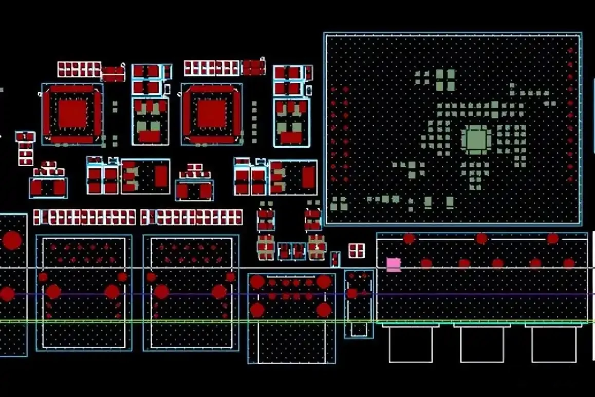
What Makes PCB Component Placement the Most Critical Stage in PCB Design?
Component placement in PCB design is the single stage where every downstream outcome is set simultaneously: signal paths, thermal zones, EMI behavior, and assembly machine execution. Routing works within the constraints that placement establishes. It cannot override them.
Placement Is Architecture, Not Arrangement
Many design teams treat placement as preparation for routing. In practice, placement is the architectural decision that all routing must serve.
When you place components, you are locking in:
- Whether critical high-speed signals can travel short, direct paths within a single reference plane
- Where thermal hotspots will form under real operating load
- Whether EMI partitioning is physically achievable
- Whether the pick-and-place machine can execute the design accurately at the production scale
None of these outcomes can be recovered through routing. A decoupling capacitor sitting 15mm from its IC power pin cannot be routed into compliance. Two high-TDP processors sharing a corner cannot be thermally separated by trace width choices. The physical arrangement decides these outcomes. Routing inherits them.
The Cost Multiplier of Late Discovery
The further a placement error travels through the design process, the more expensive it becomes. This is measurable at every stage of PCB production.
| Stage Where Problem Is Found | Correction Cost | Time Impact |
|---|---|---|
| During placement review | Engineer hours only | Hours to 1 day |
| Stage Where the Problem Is Found | Scrap batch + redesign + new prototype run | 2–4 weeks |
| Post-qualification | Re-test, re-documentation, re-submission | 4–8 weeks |
| In the field | Recall, redesign, liability exposure | Months + significant financial impact |
A placement error caught before any file is released costs almost nothing. The same error found after qualification is already embedded in production files, BOM commitments, and possibly regulatory submissions. Fixing it means restarting several stages.
The decision to invest in a rigorous placement review — whether internal or through a manufacturing partner who validates layout against real factory process parameters — pays for itself on the first production run it prevents from failing.
Understanding why placement carries this weight requires understanding what the correct placement sequence actually looks like, and what each tier controls.
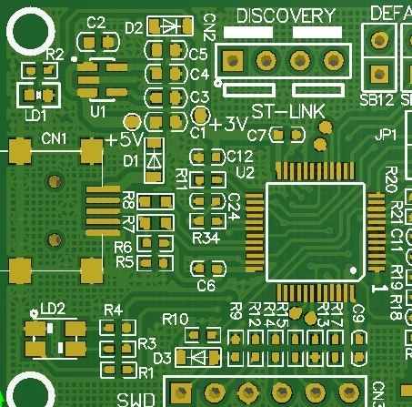
What Is the Right Sequence for PCB Component Placement, and Why Does Order Matter?
Effective PCB component placement follows four tiers: mechanically constrained parts first, then major ICs, then support components, then passives. Skipping a tier or placing components opportunistically forces routing compromises that cannot be resolved without moving parts.
Place components in the wrong order and you spend the routing stage undoing placement mistakes. The sequence is not a stylistic choice — it is a dependency chain where each tier sets the constraints the next tier must respect.
Tier 1 — Lock the Mechanical Anchors First
Connectors, power jacks, USB ports, HDMI interfaces, mounting holes, and any component defined by the enclosure or interface standard are placed first and locked immediately.
These are not design choices. The enclosure drawing or the customer’s mechanical specification defines where they go. Every other component must work around these positions.
Two critical sub-decisions belong at this tier:
ESD and transient protection must sit at the connector entry point — not downstream. A TVS diode placed even 3–5mm downstream from the connector pin allows a transient event to travel into board traces before the clamp responds. Protection must be the first thing a signal encounters when it enters the board.
Input power filtering belongs before the first switching stage. A common-mode choke or EMI filter placed after a switching regulator filters noise that has already entered the distribution network. It must sit between the power entry point and the switching stage — not after it.
With the board’s mechanical anchors locked, the routing geometry for all critical paths is now partially defined. The next tier builds directly on this foundation.
Tier 2 — Position High-Power and High-Speed ICs
Processors, FPGAs, power management ICs, DDR memory, clock generators, and RF transceivers are placed next. This is where the board’s functional zones take physical shape.
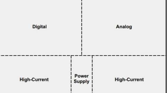
Each zone — analog, digital, power, RF — must be a defined physical region with clear boundaries. Components do not go at zone boundaries. They go inside the zone they belong to. Once zones are established, all cross-domain signal routing must pass through controlled crossing points — not across open shared copper.
| Component Type | Placement Priority | Primary Concern |
|---|---|---|
| Processor / FPGA | Adjacent to the processor | Thermal spread, routing access on all sides |
| Power management ICs | First in the power zone — near the power entry | Switching loop area, isolation from analog zone |
| DDR / high-speed memory | Adjacent to processor | Matched-length routing feasibility |
| Clock generators | Shielded, close to driven device | Short distribution path, harmonic isolation |
| RF transceivers | Isolated RF zone | Cross-domain coupling, clean antenna routing |
The key question at this tier: does the arrangement create routing geometry where critical signals stay short, remain within one reference plane layer, and do not cross zone boundaries or plane splits? If not, the components need to move before a single trace is drawn.
Once the major ICs are locked, their support components can be placed with precision. Attempting to place decoupling capacitors before knowing where IC power pins land is working in the wrong direction.
Tier 3 — Place Auxiliary Support Components
Decoupling capacitors, bulk capacitors, crystal filters, termination resistors, and ferrite beads follow the major ICs.
Decoupling capacitors: Place within 1–2mm of the IC’s power pins. The loop area formed by the capacitor, the power pin, and the ground return via must be as small as possible. Every extra millimeter of trace adds parasitic inductance that slows the transient response. At switching frequencies above 100MHz, a 100nF capacitor placed 8–10mm from a power pin provides almost no useful high-frequency decoupling.
Use two capacitor values in parallel: 100nF (0402 or 0201 package) for high-frequency response and 10µF for lower-frequency stabilization. Total bulk capacitance on any rail should be 2–10× the sum of all local decoupling on that rail. For BGA devices, via-in-pad technology places decoupling directly under the package — eliminating even the short trace distance between pad and component.

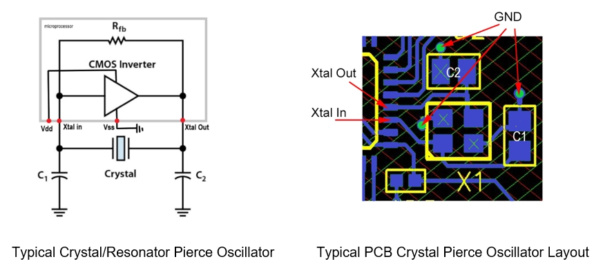
Crystal oscillators: Place directly adjacent to the driven device. Long clock traces act as antennas. A ground ring around the oscillator circuit is standard practice, not optional.
Termination resistors: Place at the driver for source termination or at the receiver for parallel termination, depending on the signal standard. This is an active design decision with defined electrical consequences — not a default.
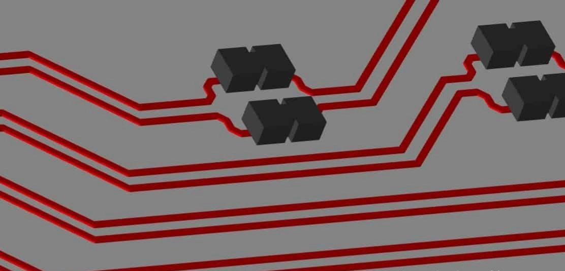
With Tier 3 complete, only passives remain. Their electrical position matters less — but their orientation consistency directly determines assembly quality.
Tier 4 — Place Passives in the Remaining Structure
Resistors, small signal capacitors, and general passives are placed last. Uniform orientation of the same component type — all same-value resistors at the same rotation, all capacitors with pin 1 in the same direction — allows the pick-and-place machine to execute repetitive placements without reconfiguration between components.
Component orientation errors account for approximately 20% of PCB assembly failures. Nearly all are preventable at this placement stage through consistent footprint orientation before files are released.

With the full placement sequence established, the next question is what goes wrong electrically when any step in this sequence is executed without discipline — starting with the failure mode that is hardest to diagnose after the board is built.
How Does Wrong Component Placement Destroy Signal Integrity?
Signal integrity problems are invisible until the board exists. Then they appear as timing failures, intermittent errors, and EMC non-compliance. Every one of them traces back to a physical decision made during placement — not routing.
Poor placement forces high-frequency return currents into detour paths that radiate EMI, create reflections, and couple noise into adjacent signals. These outcomes are structural. Routing refines signal quality; it cannot create it when the physical layout works against basic electromagnetic principles.
Return Currents Follow the Layout You Give Them
Every signal has a return current. At high frequencies, that current travels on the ground plane directly beneath the signal trace — the path of least inductance, not least resistance.
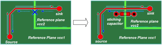
If a component’s position forces a trace to cross a gap or split in the reference plane, the return current cannot follow beneath the trace. It detours around the gap. That detour creates a current loop. The loop radiates. The larger the loop, the stronger the radiation, and the more susceptible every adjacent circuit becomes.
A trace can avoid a plane split only if the component on the receiving end is positioned to make that route geometrically possible. Placement upstream either enables or prevents a clean return path. No routing technique substitutes for a floorplan that gets this right.
Differential Pairs and Length Matching
Differential signaling — USB, HDMI, DDR, Ethernet, PCIe — relies on both traces carrying equal-amplitude, opposite-phase signals. Any length mismatch introduces skew that degrades the common-mode rejection these interfaces depend on.
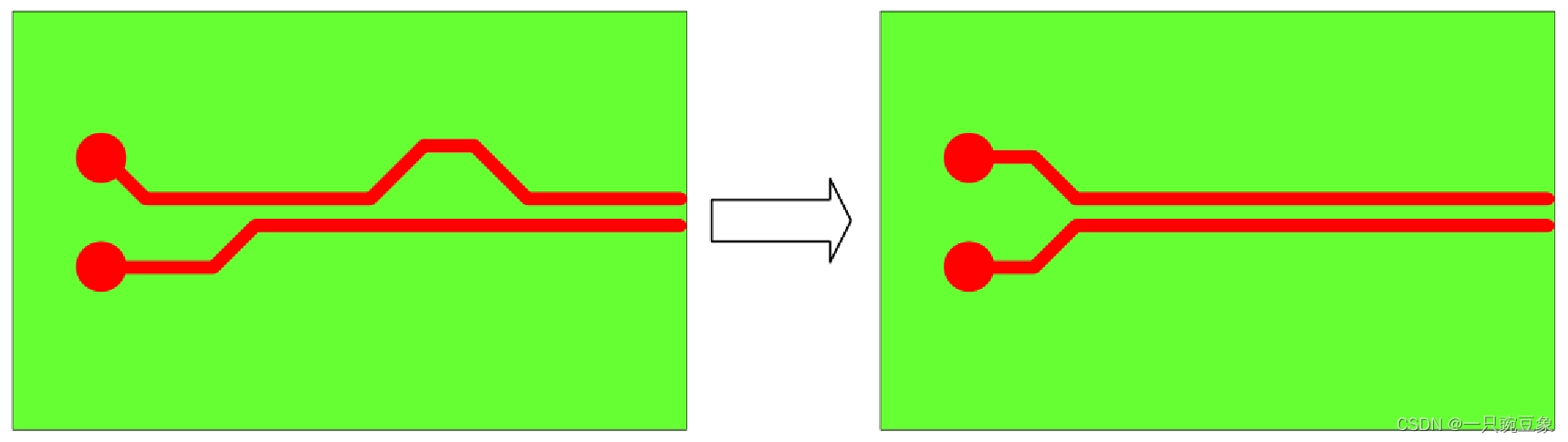
DDR4 data group length matching is typically within ±25–50 mils per byte lane. PCIe differential pairs often require ±5–10 mils. These tolerances are achievable — but only when the transmitting and receiving ICs are positioned so that matched routing is geometrically possible.
If placement forces one trace to navigate around a component the other trace does not encounter, achieving a match requires heavy serpentine tuning — which adds parasitic inductance and capacitance of its own. Good placement eliminates the need for excessive compensation. Poor placement makes it unavoidable, and sometimes makes it geometrically impossible within the tolerance band.
EMI Partitioning Is a Placement Decision
Most EMI compliance failures are not routing failures. They are partitioning failures decided at the placement stage.
Switching regulators generate broadband noise. Digital clocks generate harmonics at every multiple of their fundamental frequency. If these components sit adjacent to precision analog circuits, the noise couples into those circuits through shared planes and radiated fields — regardless of how carefully the traces are routed.
The fix is zone separation established at the floorplan stage, before any trace is drawn. Switching loop area — the enclosed path formed by the power stage, input capacitor, and output capacitor — must be minimized by placement. A compact switching loop radiates far less than a spread-out one. Rerouting traces around this loop after the fact does not reduce the loop’s radiated field.
Signal integrity is a placement outcome first. Routing refines it within the boundaries of placement sets.
That said, signal integrity is not the only failure mechanism placement governs. The second one operates slowly and invisibly — and it is often not discovered until units are already in the field.
How Does PCB Component Placement Drive Thermal Failures Nobody Sees Coming?
A board that passes every qualification test can still fail at month 14. When it does, the cause is almost always accumulated thermal stress — and that stress was built into the layout at the placement stage.
Heat accelerates every failure mechanism in electronics. A sustained 20°C increase in operating temperature can reduce a component’s expected service life by half. Placement determines where heat accumulates and where it dissipates. Decisions that create hotspots create statistically certain failures — they simply take time to appear.
How do thermal hotspots form?
Two high-TDP components placed near each other produce overlapping thermal fields. The local board temperature rises higher than any individual device’s thermal model predicts when that device is modeled in isolation.
An isolated processor running at 85°C junction temperature might reach 105°C or higher when placed next to a power management IC generating 80°C of local ambient heat. The Arrhenius relationship quantifies this precisely: every 10°C increase in junction temperature approximately doubles the failure rate for electrolytic capacitors and accelerates oxide wear in CMOS devices.
This does not appear in a standard qualification test. It appears in the 12–18 month field return window — after thousands of units are in customer hands, operating in enclosures that are warmer than the test bench and under heavier sustained load than the qualification profile covered.
Placement Decisions That Protect Thermal Margins
| Thermal Placement Rule | Risk If Ignored |
|---|---|
| Separate high-TDP components | Thermal fields overlap; junction temps exceed individual device predictions |
| Isolate precision references and oscillators from heat sources | Frequency and accuracy drift under thermal load; field-observable failures |
| Keep heat sink attachment areas physically clear | Heat sink cannot be applied without a design revision |
| Use thermal vias and copper pours under hot components | Heat stays localized; laminate delamination risk increases over time |
| Consider board mounting orientation early | Horizontal mounting limits convection — harder to manage thermally |
A processor placed under a capacitor cluster cannot receive a heat sink without a full design revision. If a component requires an external thermal solution, its placement must leave the top surface accessible — before routing begins, not after.
Precision voltage references, crystal oscillators, and low-noise amplifiers belong in the coolest region of the board, away from switching regulators and processors. For vertically mounted boards, a minimum 20mm board-to-board clearance is commonly required to prevent thermal stacking between adjacent boards in an enclosure stack.
Thermal management is a long-game problem — one that placement either solves early or defers expensively to the field. But there is a third category of placement-driven failure that does not wait months to appear. It shows up the moment the board reaches the assembly line.
What Does Your PCB Layout Need to Satisfy the Component Placement Machine?
A layout that is electrically sound and thermally well-managed can still fail at the assembly stage. The PCB component placement machine executes exactly what the design files specify. Errors in those files become production defects at scale — and at volume, scale makes everything more expensive.
Modern pick-and-place machines achieve placement accuracies of ±0.05mm and throughputs exceeding 50,000 CPH. But that performance depends entirely on design files that are clean, consistent, and DFM-compliant. Those conditions are set by the layout — not the assembly line.
How the Pick-and-Place Machine Reads Your Design?
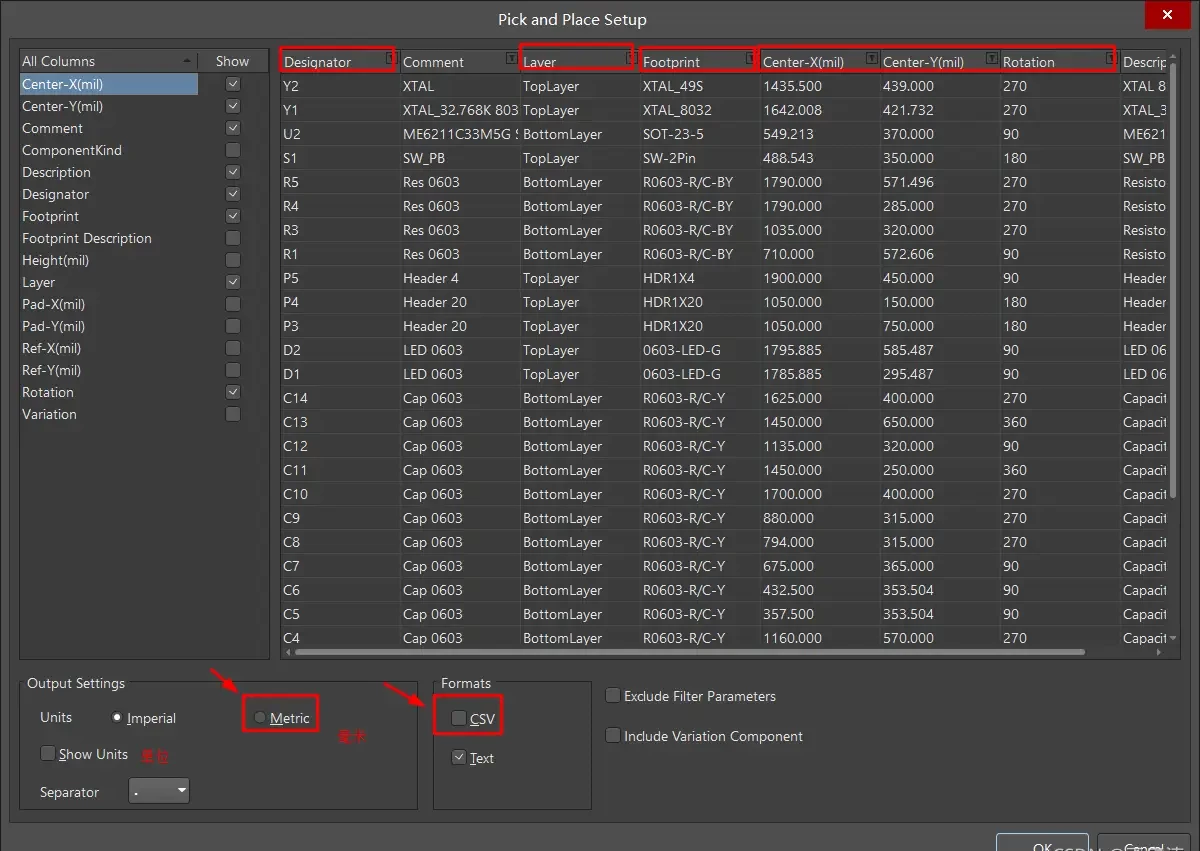
The PCB component placement machine reads a centroid file — also called an XY or pick-and-place file — specifying each component’s X-Y coordinate and rotation angle. It retrieves components from tape-and-reel feeders using vacuum nozzles, aligns them using high-resolution vision systems, and places them onto solder-paste-coated pads.
High-volume chip shooters exceed 50,000 CPH. Precision placers handling fine-pitch BGAs and 01005 passives operate at 10,000–20,000 CPH with accuracies reaching ±20–40µm. Real-world throughput runs 15–30% below rated CPH due to board complexity, feeder switching, and component variation.
Any error in the centroid file — wrong rotation, wrong coordinate, wrong layer assignment — becomes a placement defect. It may not cause immediate failure. It commonly manifests as a marginal solder joint or elevated contact resistance that surfaces under thermal cycling or vibration stress — one of the hardest failure modes to trace in field returns.
The DFM Rules That Are Set at Placement, Not Routing
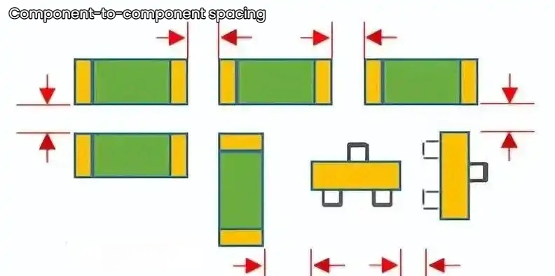
Component-to-component spacing. IPC-2221A defines baseline spacing requirements between adjacent component bodies. A practical DFM minimum for standard SMD assembly is 0.5mm between component bodies. Spacing violations cause solder bridging during reflow and block AOI access to component leads. These spacings are defined by placement — no routing adjustment compensates for components placed too close together.
Wave solder orientation. For through-hole and mixed SMD/THT boards, component orientation relative to the wave solder travel direction determines whether downstream pads are shadowed from solder contact. Shadowed pads produce solder-starved joints that pass visual inspection but fail under mechanical or thermal load. This is a placement decision with no assembly-stage fix.
Fiducial marker keep-out zones. Fiducials are the optical reference targets the machine uses to calibrate board coordinate origin. Components placed inside a fiducial’s keep-out zone prevent accurate vision alignment — and every subsequent placement on that board degrades in accuracy from that point forward.
Test point availability. ICT fixtures probe testable nets on the board’s underside. If placement leaves no routing path for test points on critical nets, ICT cannot validate the assembled board. This is discovered after fabrication and assembly — forcing a design revision or accepting reduced test coverage.
What the Yield Data Shows
Designs without DFM validation at the placement stage consistently produce first-run yields below 80%. Designs reviewed against IPC standards and factory process parameters before release consistently reach 95–98% first-run yield. On a production run of 10,000 units, the difference between 80% and 97% is more than 1,700 defective boards requiring rework or scrap. A proper DFM review at the placement stage recovers that cost on the first batch.
Understanding placement from the assembly machine’s perspective applies to most boards. But for regulated industries — automotive, medical, industrial — placement carries an additional layer of requirements that cannot be satisfied through routing or assembly process control if the layout is already wrong.
Does Your Industry Change the PCB Component Placement Rules You Must Follow?
General placement best practice covers most boards. But regulated industries add requirements that are not optional — and some of them are impossible to satisfy through routing or process control if the placement decision was already made incorrectly.
Industry-specific placement requirements exist because the failure modes these boards must survive — and the consequences of those failures — are fundamentally different from a standard commercial electronics design.
Automotive: Safety Architecture and Component Qualification
Automotive PCBs must survive continuous vibration, temperature cycling from −40°C to +125°C, and electromagnetic environments generated by high-current motor drives and ignition systems.
ISO 26262 functional safety requirements impose a placement discipline that most commercial designs never encounter: redundant circuit elements must be physically separated. A placement decision that consolidates redundant paths for routing convenience can violate the spatial separation requirement of the safety architecture — and that is a qualification non-conformance, not a design preference.
AEC-Q100 component qualification grades define temperature limits. A Grade B component (−40°C to +105°C) placed in a zone where junction temperature reaches 115°C under worst-case load is a qualification violation. It will not fail in the test lab at standard qualification temperatures. It will fail in service — in the specific vehicles where that zone runs hottest.
Medical: Class 3 Assembly and Zero-Tolerance Reliability
IPC-A-610 Class 3 — required for life-support and implantable devices — imposes placement constraints on component spacing, pad geometry, and orientation that directly affect solder joint formation. These are not guidelines. Non-conformance at the assembly stage is a regulatory issue.
ISO 13485 and FDA 21 CFR Part 820 traceability requirements mean every component lot, every soldering parameter, and every inspection record must be traceable to the specific board. The assembly process must structurally support that documentation chain — and the placement must support the assembly process that generates it.
Over 40% of medical device companies experience product launch delays or regulatory complications directly attributable to PCBA non-compliance. In most cases, the root cause is in placement and DFM decisions that were not made with the assembly standard in mind.
High-Voltage Industrial: Creepage and Clearance Are Placement Rules
For industrial boards above 50V, creepage (surface distance) and clearance (air gap) requirements between conductors are defined by IEC 60950, IEC 62368, and applicable safety agency standards.
These are not routing constraints. They are placement constraints. If a high-voltage component and a low-voltage component are placed too close together, no routing solution achieves the required isolation distance. The only fix is moving one of the components — which, if the board is already fabricated, means a new design revision and schedule impact.
The pattern across all three industries is consistent: the placement stage is where compliance is determined. Testing verifies it. Testing cannot create it.
Can a One-Stop PCB Partner in China Close the Gap Between Design and Production?
The most persistent source of placement-related production problems is the gap between the designer and the manufacturer. When these two parties are separate organizations, placement is optimized for what the schematic requires — not for what the factory’s specific equipment, process parameters, and quality standards can actually execute.
This is not a hypothetical problem. It is the default condition for most overseas buyers sourcing PCB design and manufacturing from separate vendors.
Why the Design-to-Production Gap Creates Placement Failures?
A PCB designer working independently has no direct visibility into the production environment. They do not know:
- What pick-and-place machine will handle the board, or its specific accuracy and feeder configuration
- What reflow oven profile will be used, and how the board’s thermal mass affects actual component temperatures during soldering
- What DFM rules the specific factory enforce for component spacing, orientation, and test point access
- Which components in the BOM have lead time problems that may require a footprint adjustment for an alternative package
These factors change what a “correct” placement looks like. A design that is technically compliant with IPC standards can still generate assembly problems on a specific line if it was designed without knowledge of that line.
What Integration Between Design and Production Changes
At IWDF Solutions, our PCB design engineers work in the same facility as our manufacturing and assembly teams in Shenzhen. When our engineers place components, they have direct knowledge of the SMT line’s equipment specifications, the reflow oven’s zone profiles, the AOI and X-ray inspection systems’ resolution limits, and the DFM rules enforced at our specific process capability level.
Placement decisions that would cause yield loss on a poorly matched line are caught before the design file is finalized — not after the first production batch.
For clients who already have a design, our DFM review evaluates every component placement decision against our factory’s process parameters before fabrication begins. For clients who need PCB reverse engineering — to reproduce an obsolete design or modernize a legacy product — our team reconstructs the layout with updated placement that reflects current DFM standards and component availability.
For clients going from concept to volume production, our one-stop service covers PCB design, PCB reverse engineering, PCB manufacturing, and PCBA production — with placement validated against production reality at every stage.
If you are evaluating whether your current design is production-ready, or looking for a PCB design and manufacturing partner that delivers volume-quality results from the first prototype, contact IWDF Solutions. Our engineering team responds with a technical assessment — not a template quote.
FAQ: PCB Component Placement — Questions Engineers and Buyers Actually Ask
What is PCB component placement, and why does it matter?
PCB component placement is the physical arrangement of every electronic component on a printed circuit board. It determines signal path quality, thermal distribution, EMI behavior, and assembly yield — before routing begins. Poor placement cannot be corrected by routing. It determines production outcome from the start.
How close should decoupling capacitors be to IC power pins?
Within 1–2mm is the practical target for high-speed designs. The shorter the path, the lower the parasitic inductance, and the faster the capacitor responds to switching transients. For BGA devices, via-in-pad placement directly under the package eliminates even that short distance. Full technical detail is covered in the Tier 3 placement section above.
What is the minimum spacing between components on a PCB?
IPC-2221A defines baseline spacing by component type and assembly class. A practical DFM minimum for standard SMD assembly is 0.5mm between component bodies. Fine-pitch BGAs and mixed SMD/THT boards carry additional requirements. Always verify spacing against the assembly standard applicable to your board’s end-use environment.
Can routing fix a bad component placement?
No. Routing works within the constraints placement sets. If a component is placed in a position that forces critical signals across split planes, creates unresolvable thermal interactions, or violates isolation distances, no routing technique provides a solution. The component must move.
What is a PCB component placement machine, and how does it affect my design?
A pick-and-place machine reads centroid files and places each component onto solder-paste-coated pads using vacuum nozzles and vision alignment systems. Your design’s component orientation consistency, centroid data accuracy, fiducial marker placement, and component spacing directly determine whether the machine can execute the assembly accurately and at full production yield.
What placement rules are different for automotive PCBs?
ISO 26262 requires physical separation of redundant safety-critical circuits. AEC-Q100 qualification grades must match the actual thermal environment at each component’s placement location. Vibration resistance and electromagnetic compatibility requirements impose additional constraints that standard commercial design rules do not cover.
How does component placement affect PCB assembly yield?
DFM-compliant placement consistently produces first-run yields of 95–98%. Designs without DFM validation at the placement stage typically produce yields below 80%. On any significant production volume, that gap translates directly into rework cost, scrap cost, and schedule delays.
What is PCB reverse engineering, and when should I consider it?
PCB reverse engineering reconstructs a physical board into full design documentation — Gerber files, BOM, schematic, and placement data — from the physical hardware. It is used when original design files are lost, when a legacy product must be re-manufactured with updated components, or when a design needs performance improvements that require layout-level access.
How does IWDF Solutions handle component placement for overseas clients?
IWDF Solutions integrates PCB design and PCB manufacturing in one facility in Shenzhen. Our design team places components against our factory’s specific process parameters — pick-and-place machine specifications, reflow profiles, DFM rules, and current component availability. Every design receives a DFM review before fabrication begins. Clients receive production-validated files, not just schematic-compliant files.

