
When you’ve decided to use a PCB reverse engineering service, now come the harder questions: What will you actually receive? How does the process work from your side? Is the quotation from the supplier high or not? How do you tell a capable engineering partner from one who will waste your time and money?
A PCB reverse engineering service supplier takes a physical circuit board and reconstructs its complete design documentation — Gerber files, schematics, BOM, and editable CAD files — from scratch—no original data required. The output is a full, manufacturable file package you can use to reproduce, modify, or improve the board.
But knowing what the service does is only the beginning. Before you contact a single supplier, you need to know what deliverables to request, how the process works on your side, what to prepare, what it costs range is, and how to tell a serious engineering partner from one that will waste your time. This guide covers all of it — in the order you actually need it.
What Is a PCB Reverse Engineering Service?
You have a board with no PCB documentation and no original designer. Now you need to repair, upgrade, reproduce, or modify it. But most engineers don’t have the tools, materials, components, time, or experience to do this in-house — that’s what the service is for.
A PCB reverse engineering service is a professional technical service where engineers analyze a physical circuit board and reconstruct the full design package. The output gives you everything you need to manufacture, modify, or understand the board — even when no original design data exists.

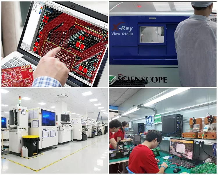
This is not the same as DIY reverse engineering, where someone manually traces connections with a multimeter and sketches a schematic by hand. A professional service uses industrial equipment — high-resolution scanners, X-ray machines, CT scanners, and professional EDA software — to do this work accurately and at scale.
Situations That Make This Service the Right Call
| Scenario | The Real Problem | What Reverse Engineering Solves |
|---|---|---|
| Critical component has gone EOL | A key IC or chip on the board has reached end-of-life (EOL). You can no longer source it from any distributor. Every time a board fails or wears out, you lose one more machine — until eventually the equipment can’t be kept running at all. | Recover the full design, identify the obsolete component, and update the BOM with a functional modern replacement — so the board can be reproduced and the equipment keeps running |
| Original PCB supplier stopped or raised prices | The factory that made your board shut down, stopped accepting orders, or quoted a price you can’t justify. You need a new manufacturer — but you have no Gerber files to hand them. | Reconstruct the complete file package (Gerbers, BOM, drill files) so you can immediately qualify a new, more cost-effective supplier |
| A board failed inside the equipment | A specific PCB inside a high-value machine has burned out or broken. Replacing the entire machine costs tens of thousands of dollars. The failed board alone is no longer available to buy. | Reverse engineer the failed board, reproduce it, and restore the machine to full operation at a fraction of the replacement cost |
| You acquired a product with no design documentation | Through a company acquisition, asset purchase, or staff turnover, you now own a product in production — but no design files came with it. You can’t modify, scale, or re-source the boards without them. | Reconstruct the full design baseline so you can hand files to any manufacturer, make engineering changes, and take full control of your own product |
If your situation matches one of these, you are a natural candidate for this service.
What Can You Get from a PCB Reverse Engineering Service?
Most buyers will receive “the files.” But what files, exactly? The answer varies between providers — and if you don’t ask upfront, you may get far less than you actually need.
A complete PCB reverse engineering service delivers Gerber files, NC Drill files, a full schematic, a Bill of Materials, and editable CAD layout files compatible with software like Altium Designer or KiCad. Some providers also include a functional validation report and assembled prototype boards as part of the package.
What Each Deliverable Does — and Why It Matters
| Deliverable | What It Contains | Why You Need It |
|---|---|---|
| Gerber Files | Copper traces, solder mask, silkscreen for every layer | Required to fabricate the bare PCB at any manufacturer |
| NC Drill Files | Drill hole locations, sizes, and types | Required alongside Gerbers for board fabrication |
| Schematic | Full circuit diagram showing component connections | Required for design modifications, troubleshooting, and compliance documentation |
| BOM (Bill of Materials) | Component list with values, packages, and part numbers | Required for component sourcing and assembly |
| Editable CAD Layout File | PCB layout in Altium, KiCad, PADS, or Eagle | Required if you ever need to modify the design later |
| Pick-and-Place File | Component X/Y coordinates, rotation, and placement side | Required for automated SMT assembly |
| Test and Validation Report | Functional verification results from a prototype build | Confirms the reconstructed files produce a working board |
Not every provider delivers all of these by default. Some give only Gerber’s and a BOM. Others include full schematics and editable CAD files. Before you request a quote, decide which files you actually need and state that clearly. If you ever want to modify the design — not just reproduce it — you need the editable CAD files. Gerbers alone won’t give you that flexibility.

How Does the Process Work? A Step-by-Step Overview
Sending a board to a service provider can feel like handing off a black box. So you need to know what happens at each step — and, more importantly, what your own responsibilities are at each stage.
The PCB reverse engineering process runs from sample submission through feasibility assessment, NDA signing, internal engineering analysis, draft file review, and final delivery. Most providers also offer optional prototyping to validate the reconstructed files. From your side, the main tasks are submitting samples, reviewing deliverables, and confirming the final package.
What Happens at Each Stage
| Stage | Provider’s Role | Your Role |
|---|---|---|
| 1. Sample submission | Receives and logs the board | Ship samples with a brief description of the board’s function and your delivery requirements |
| 2. Feasibility review + quote | Evaluates layer count, component density, and technical complexity | Review the quote; ask about scope, timeline, and what’s included |
| 3. NDA + contract | Prepares the service agreement | Sign the NDA before any work begins — this protects your design IP |
| 4. Engineering analysis | Scans, disassembles, traces, and reconstructs the design | Wait; a good provider gives progress updates at key milestones |
| 5. Draft file delivery | Sends the initial file package for your review | Review the files against the physical board or any existing documentation |
| 6. Revision + final delivery | Addresses corrections and finalizes all files | Confirm all files are in your required formats before final sign-off |
| 7. Prototyping (optional) | Fabricates and assembles a board from the reverse-engineered files | Inspect and test the prototype to validate accuracy |
The optional prototyping step is worth paying for. A prototype built from the reverse-engineered files is the only reliable way to confirm everything is correct before you commit to a production run.
What Should You Prepare Before Contacting a Supplier?
Most buyers contact dozens of suppliers to compare prices and services, but due to the limited information provided, each supplier has different requirements. This results in vague quotes, unnecessary delays, and unexpected price fluctuations. Now, a few minutes of preparation changes all of that.
Before contacting a PCB reverse engineering service provider, prepare your board samples, determine the layer count if possible, note any damage or missing components, decide which file formats you need, and identify whether any programmable chips require firmware extraction (IC decryption). This information determines cost, method, timeline — and whether a provider can take the job at all.
Five Things to Clarify Before You Write That First Email
1. How many board samples can you provide?
For non-destructive methods — X-ray or CT scanning — one sample is usually enough. For destructive methods, where the board is physically delaminated layer by layer, you should provide at least two samples. One is used for analysis. The other stays as a reference.
If you only have one board and it cannot be replaced, say so upfront. A good provider will adjust their approach to protect it, though non-destructive methods may cost slightly more.
2. Do you know the layer count?
If you don’t know, the provider can determine it through inspection — that’s fine. But stating it upfront helps them quote faster and more accurately. A rough way to check yourself: hold the board up to a bright light. If you can see traces running inside the board between the surface layers, it’s likely four layers or more.
3. Is the board damaged or incomplete?
Note any visible problems before shipping — corroded pads, missing components, burned areas, cracked traces, or erased silkscreen markings. These issues don’t disqualify a board. But the provider needs to know about them to scope the work correctly.
4. Which output file formats do you need?
Know which EDA software your team uses. State it in your inquiry. Common options:
- Altium Designer (.PcbDoc, .SchDoc)
- KiCad (.kicad_pcb, .kicad_sch)
- Mentor PADS (.pcb, .sch)
- Eagle (.brd, .sch)
- Gerber + NC Drill only — if you just need to fabricate without modifying the design
5. Are there programmable chips on the board?
If the board contains microcontrollers (MCUs), FPGAs, or DSPs, the physical layout alone is not enough to replicate full board functionality. You also need the firmware — the software programmed into those chips. Extracting it is called IC decryption or chip unlock. It adds time and cost, but it is essential when those chips control critical board functions. Identify this before you request a quote.
How to Prepare the Materials You Need to Send
You’ve identified the right supplier. Now what do you actually send them? Sending the wrong materials — or not enough of them — is one of the most common reasons projects get delayed after they’ve already started.
Along with the physical board, include any existing documentation, a clear description of the board’s function, your target deliverables, and your component sourcing preferences. Even partial information — an old product manual, a rough sketch — can cut hours off the analysis phase and reduce your overall project cost.
What to Include in Your Sample Submission Package
- Physical board sample(s) — pack in anti-static (ESD) bags with foam cushioning. For international shipments, label as “electronic circuit board sample for engineering analysis — no commercial value” to help with customs clearance.
- Any existing documentation — partial schematics, old BOMs, product manuals, datasheet printouts, or photographs of an assembled unit. Anything helps.
- Functional description — describe what the board does. Include operating voltage, key interfaces (USB, RS-232, CAN, Ethernet, etc.), and the environment it works in (temperature range, humidity, vibration).
- Target deliverables list — write out exactly which files you need and in which formats. Be specific.
- Component sourcing preferences — state whether you need exact original components or whether modern equivalents are acceptable. Many original parts have been discontinued. A good provider can identify functional alternatives and update the BOM accordingly.
How Much Does a PCB Reverse Engineering Service Cost?
Pricing for this service is not transparent. Most providers don’t publish rates. And the range between a simple board and a complex one can be enormous — sometimes 30 to 50 times the base price, depending on what’s involved.
PCB reverse engineering service cost depends primarily on layer count, component count, chip complexity, and whether IC decryption is needed. A simple 2-layer board can cost as little as $100–$500. A complex multilayer board with dense BGA components and IC decryption can run $3,000–$25,000 or more. Always ask for an itemized quote before committing.
Cost Components Broken Down
| Cost Item | Typical Range | Notes |
|---|---|---|
| Component dismantling | $50–$200 | Based on component count and board density |
| Layer polishing / delamination | $50–$150 per layer | For multilayer destructive analysis |
| PCB point tracing | $0.50–$0.60 per point | Applies regardless of layer count |
| Intermediate layer reconstruction | $100–$200 per layer | For internal layers in multilayer boards |
| Schematic reconstruction | $1.00–$2 per point | Based on schematic complexity |
| BOM compilation | $80–$500 | Higher when markings are erased or custom-coded |
| IC decryption | $300–$3,000+ per chip | Varies widely by chip type and security level |
Project-Level Pricing Benchmarks
| Board Type | Estimated Cost | Typical Turnaround |
|---|---|---|
| 1–2 layer, simple design | $100–$500 | 3–7 days |
| 4–6 layer, standard industrial board | $600–$2,000 | 5–10 days |
| 8–12 layer, complex layout | $1,500–$5,000 | 2–3 weeks |
| 16+ layer / HDI / BGA-heavy | $5,000–$15,000+ | 3–6 weeks |
| Full project (RE + prototype + production) | $3,000–$25,000+ | 3–8 weeks |
What Drives the Price Up?
- Layer count — each additional layer adds scanning, polishing, and alignment work.
- Component density — more components mean more points to trace and more items to identify in the BOM.
- IC decryption — on boards with programmable chips, this is often the single biggest cost variable.
- Turnaround time — rush orders typically carry a 20–50% premium.
- Number of output formats — producing files for two or three different EDA tools costs more than delivering one format.
- Board condition — damaged or heavily corroded boards require extra restoration work before analysis can begin.
The cheapest quote is rarely the best value. A provider that delivers incorrect Gerbers or an incomplete BOM will cost you far more in failed prototypes and production rework than a slightly higher upfront price for accurate work.
Questions to Ask Before Choosing a PCB Reverse Engineering Partner
A lot of providers look the same from the outside. The sales pitch is almost always identical. The only way to tell the difference is to ask specific technical questions — and pay close attention to the quality of the answers.
Before committing to any PCB reverse engineering service provider, ask about their maximum layer count capability, NDA policy, deliverable formats, analysis methods, turnaround time, prototyping capability, and revision policy. Specific, confident answers to these seven questions separate experienced engineering firms from low-cost operators who outsource work they don’t fully control.
The Seven Questions That Matter
1. What is your maximum layer count capability?
Make sure the provider has handled boards at your complexity level before — and ask to see examples of comparable past projects. A provider who has never worked on a 12-20 layer board should not be your first choice for one.
2. Will you sign an NDA before seeing the board? What is your IP protection policy?
Any legitimate provider will sign an NDA without hesitation. Also ask what happens to your files after the project ends — are they deleted, archived, or stored on shared servers? This matters for your long-term IP security.
3. What file formats do you deliver as standard?
Get a specific list in writing. Confirm that editable CAD files are included if you need them — not just Gerber output. “We deliver all files” is not a useful answer. “We deliver Altium .PcbDoc, .SchDoc, Gerber, BOM in Excel, and NC Drill” is.
4. Do you use destructive or non-destructive methods? How many board samples do you need?
Non-destructive methods (X-ray, CT scan) preserve the physical board. Destructive methods (mechanical delamination) give higher accuracy for complex internal layers but consume the sample. Know which method applies to your situation — and confirm the sample quantity requirement before you ship anything.
5. What is your standard turnaround time? Is expedited service available?
Get the timeline in writing as part of the contract. Also ask what happens if they miss the agreed deadline — priority escalation, or just an apology? This tells you a lot.
6. After the reverse engineering is done, can you produce prototype boards directly?
A provider who can go from reverse-engineered files to fabrication and assembly in-house eliminates the risk of file handoff errors between separate vendors. One point of contact means one point of accountability throughout the entire process.
7. What is your revision policy if the delivered files have errors?
No reputable provider should charge extra for fixing their own mistakes. Get this confirmed in writing before any payment is made.
Why Use IWDF Solutions for PCB Reverse Engineering?
There are hundreds of PCB reverse engineering service providers in Shenzhen. Most claim identical capabilities. What actually separates them is technical depth, process transparency, and what happens after the files are delivered.
IWDF Solutions is a Shenzhen-based PCB engineering and manufacturing company providing PCB reverse engineering, PCB design, PCB fabrication, and PCBA production under one roof. Your project moves from a physical board to a validated, assembled prototype — and then into volume production — without switching vendors or managing multiple contacts.
What We Can Actually Handle?
Layer capability: We handle boards from single-layer through 20+ layer HDI designs, including blind vias, buried vias, and via-in-pad configurations.
Turnaround: Standard projects are completed in 5–15 business days depending on complexity. Rush service is available for time-critical requirements.
IC decryption: We support firmware extraction for a wide range of microcontrollers and FPGAs. If your board contains programmable chips, mention it in your first inquiry — we will assess feasibility and give you a straight answer.
Industries we work with regularly:
| Industry | Typical Reverse Engineering Use Case |
|---|---|
| Industrial automation | Replacing discontinued PLC and controller boards for legacy factory equipment |
| Automotive | ECU board documentation recovery for repair programs and parts requalification |
| Medical devices | Maintaining FDA-cleared equipment when original board manufacturers are no longer active |
| Telecommunications | Replicating RF and baseband boards as part of network equipment lifecycle extension programs |
One-Stop Service: From Reverse Engineering to Production
IWDF Solutions covers the full chain in-house:
- PCB reverse engineering — reconstruct all design files from your physical board
- Design review and optimization — update obsolete components and improve the layout for modern manufacturing
- PCB fabrication — produce bare boards directly from the reverse-engineered Gerbers
- Component sourcing — source the full BOM and identify alternatives for discontinued parts
- PCBA production — SMT and DIP assembly with AOI inspection and functional testing
- Prototype delivery — validated, tested prototype boards before committing to volume
You don’t need to manage separate vendors for each of these steps. One contact, one workflow, one point of accountability.
Ready to start? Send your inquiry to IWDF Solutions with a brief description of your board, your required deliverables, and your target timeline. We’ll respond within 24 hours with a feasibility assessment and a clear quote.


Frequently Asked Questions
Can you reverse engineer a PCB without damaging the board?
Yes, for many boards. X-ray imaging and CT scanning can reveal internal layer structures without any physical damage. For boards with very dense internal routing, destructive layer separation may still produce higher accuracy. If your sample cannot be replaced, tell the provider upfront — they can adjust the method to protect it.
How accurate is PCB reverse engineering?
With the right equipment and experienced engineers, layout accuracy is very high. Gerber files and BOM lists can closely match the original design. Accuracy drops on boards with heavily erased component markings or non-standard substrate materials. Functional prototype testing is the only fully reliable confirmation of accuracy.
What if some of my components are obsolete?
This is one of the most common reasons companies use this service. A professional provider identifies obsolete components during BOM compilation and recommends modern, functionally equivalent replacements. The updated BOM can be included as a standard deliverable.
Is PCB reverse engineering legal?
Reverse engineering a board you lawfully own — for repair, maintenance, file recovery, or design modification — is legal in most jurisdictions. Reverse engineering a competitor’s patented product for commercial reproduction is not. If your situation involves any third-party IP, consult an IP attorney before starting the project.
How many board samples do I need to provide?
For non-destructive analysis, one sample is usually sufficient. For destructive analysis (physical delamination), two samples are strongly recommended. If you only have one irreplaceable board, tell the provider before shipping anything and ask them to use non-destructive methods only.
Do I need IC decryption for every board?
No. IC decryption is only necessary when the board contains programmable chips — microcontrollers, FPGAs, DSPs — whose firmware controls critical functionality. Boards using only passive components, standard analog ICs, or logic gates do not require IC decryption.
How do I ship my board to a provider in China?
Use a reputable express courier such as DHL, FedEx, or UPS with a tracking number. Pack the board in an anti-static (ESD) bag with firm foam cushioning. For customs purposes, describe the item as “electronic circuit board sample for engineering analysis — no commercial value.” This description minimizes the risk of customs delays or inspections.
What is the difference between PCB reverse engineering and PCB cloning?
PCB reverse engineering focuses on reconstructing the design with the intent to understand and potentially improve it — updating obsolete components, fixing layout issues, or optimizing for a new manufacturing process. PCB cloning is a 1:1 replication of the original layout without modification. Both start from the same physical board. The difference is what you do with the output.
Conclusion
PCB reverse engineering is not complicated in concept. A physical board goes in. A complete, manufacturable file package comes out. But the quality of that output depends entirely on the skill of the provider and the clarity of the brief you give them.
Before you start: know what deliverables you actually need, prepare your samples correctly, ask the seven questions above, and make sure an NDA is signed before any information leaves your hands.
If you want a single partner who can take a board from reverse engineering all the way through to a tested, assembled prototype — and then into full production — IWDF Solutions handles that entire chain from one facility in Shenzhen. Send us your inquiry and we’ll tell you exactly what we can do, how long it takes, and what it costs.

