

What Is AI Auto Routing in PCB Design?
PCB auto routing has been around for decades, but traditional autorouters were relatively simple: given a list of connections (netlist) and a set of design rules, they would attempt to find the shortest path between pins, layer by layer, trying to avoid collisions. The results were often disappointing—messy routing, excessive vias, and lots of manual cleanup work afterward. Most experienced designers learned to distrust them entirely.
Modern AI-powered auto routing is fundamentally different. Instead of blindly searching for paths, contemporary AI tools apply machine learning, reinforcement learning, or physics-based algorithms to understand your design intent, anticipate signal integrity challenges, consider manufacturing constraints, and generate routing that doesn’t just connect dots—it optimizes for performance, manufacturability, and cost.
The best AI routing tools work in one of three ways:
First, integrated AI-assisted routing, where a mature EDA vendor like Altium or Cadence embeds AI suggestions into its existing environment. Your design rules, constraints, and previous successes inform the AI. You remain in control.
Second, cloud-native autonomous routing, where dedicated platforms like DeepPCB or Quilter accept your design files and generate complete layouts in minutes using pure AI, returning fabrication-ready Gerber files.
Third, physics-driven automation, exemplified by Quilter, which trains reinforcement learning models on fundamental electromagnetic and thermodynamic principles rather than human patterns—discovering solutions no engineer would have tried.

Who Should Use AI Auto Routing?
AI auto routing is genuinely valuable when used appropriately. You should consider it if your team faces one or more of these scenarios:
Good use cases: Prototype development on simple to mid-complexity boards, repetitive designs with minimal variation, tight time-to-market requirements, distributed teams that lack in-house layout specialists, educational and research projects needing fast iteration, or low-to-medium density digital boards where standard routing practices work well.
The real time savings emerge when you move from “three days of manual routing” to “30 minutes of automated placement and routing plus 2–3 hours of engineer review.” For a startup shipping its fifth revision, that acceleration is game-changing.
Who Should Not Use AI Auto Routing?
AI auto routing has firm limitations. If your project involves high-speed differential interfaces (USB 3.1, PCIe, 10 Gbps Ethernet), extremely dense BGA fanouts with HDI requirements, mixed-signal analog-to-RF integration with strict isolation needs, or specialized requirements like automotive-grade reliability (AEC-Q standard) or aerospace qualification, you need experienced human judgment for critical signal paths. AI can assist, but it cannot replace an engineer’s understanding of your application’s physics.
Similarly, if your design requires custom impedance structures, complex power delivery networks with multiple voltage domains, or exotic layer stackups, AI will struggle without extensive manual constraint definition—and at that point, a skilled layout engineer might actually be faster.
Key Criteria to Evaluate AI Tools for PCB Auto Routing
Before you choose a tool, understand what matters most for your workflow.
Routing Quality and DRC/DFM Awareness. Can the tool enforce your design rules—trace width, spacing, via size, layer usage—and also understand manufacturing constraints? A tool that generates beautiful, rule-compliant routing but ignores your PCB manufacturer’s capabilities will cause problems at fabrication. Does it support layer-to-layer impedance control? Can it automatically verify that your design is printable?
Support for High-Speed and Multi-Layer Design. If your board has differential pairs (USB, HDMI, Ethernet), can the tool maintain consistent spacing and length matching? Does it understand DDR timing constraints or long trace requirements for clock distribution? Can it handle 6, 8, or 10-layer stackups with power planes and multiple ground planes?
Integration with Your Existing EDA Stack. Are you locked into Altium Designer? Do you use Cadence Allegro at your company? Do you prefer the open-source KiCad ecosystem? Some AI routing tools operate independently (you upload files, get back Gerbers), while others are tightly integrated into your existing CAD environment. That choice affects your workflow efficiency.
Cloud, Collaboration, and IP Security. Will your design data be stored on someone else’s servers? Does the tool use your designs to train its AI model? This matters for companies with confidential hardware. Some vendors (like Quilter) explicitly promise that customer designs are never used for AI training. Others operate fully on-premise or in your private cloud.
Vendor Support and Ecosystem Maturity. Is the tool maintained by a stable company with a multi-year roadmap? Can you get technical support when something breaks? Are there active user communities sharing tips and workarounds?
10 Best AI Tools for Auto Routing in PCB Design (2026)
Comparison Table: AI Auto Routing Tools Overview
| Tool Name | Positioning | Key Strength | Layer Support | Primary Integration | Best For | Price Model |
|---|---|---|---|---|---|---|
| Altium Designer (with AI) | Integrated AI assistant | Rule-driven, familiar EDA, strong DFM | Up to 32 | Native (Altium) | Established design teams | Subscription ($2,500+/yr) |
| Cadence Allegro X AI | Generative AI for placement & routing | Evaluates 1000s of strategies, DFA/DFM constraints | Unlimited | Native (Cadence) | Complex, high-performance designs | Subscription (custom pricing) |
| DeepPCB | Pure AI cloud platform | Fully autonomous, DRC-clean results, fast | Up to 8 | Standalone cloud | Prototypes, quick iteration, cost-sensitive | Pay-per-use ($50–500/design) |
| Flux (with AI Copilot) | Browser-based collaborative ECAD + AI | Real-time collaboration, sourcing-aware, beginner-friendly | Up to 8 | Standalone cloud/browser | Startups, distributed teams, agile hardware | Subscription ($15–49/mo + AI credits) |
| Quilter | Physics-driven autonomous layout | Truly autonomous, physics-validated, multi-candidate generation | Up to 8 | Standalone (exports to Altium/Cadence/KiCad) | Complex designs, optimization-focused, competition in time | Subscription or usage-based (custom) |
| Keysight EDA (with AI/ML) | Simulation-first AI integration | AI-optimized circuit models, signal/power integrity analysis | Flexible | Native (Keysight) or export | High-speed, RF, power integrity–first designs | Subscription (custom pricing) |
| KiCad + AI Automation (Autocuro, Huaqiu) | AI layer on open-source | Free/open base, schematic-aware routing, local IP security | Up to 8 | KiCad native via Python scripting | Budget-conscious teams, open-source preference | Free or low-cost ($0–200/mo add-on) |
| Autodesk Fusion 360 (Eagle + AI Assist) | Cloud ECAD with assisted routing | Mechanical-electrical co-design, interactive routing help | Up to 16 | Native (Fusion 360) | Mechatronic devices, parametric designs | Subscription ($460/yr personal, custom enterprise) |
| Zuken (e.g., CR-8000) | Enterprise PCB design & optimization | Advanced constraint-driven layout and optimization for complex, high-speed systems | Unlimited (tool-dependent) | Native (Zuken ecosystem) | Large teams, complex multi-board/high-speed designs | Enterprise subscription (custom pricing) |
| General-Purpose GenAI (ChatGPT, Claude, Gemini) | Design rule & workflow assistant | Rapid constraint rule generation, DFT planning, design review scripts | N/A | External | Learning, constraint drafting, automation scripting | ChatGPT Plus ($20/mo), Gemini Free/Pro, Claude varies |
Tool 1: Altium Designer with AI-Powered Routing Suggestions
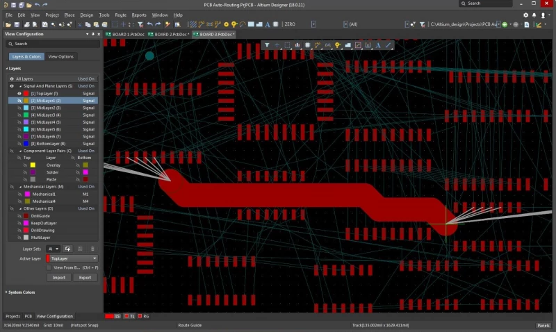
Altium remains the dominant professional PCB design platform in the US and Europe. Its autorouter has been refined over 20+ years, and in recent versions, Altium has begun layering AI suggestions into the routing workflow. The AI doesn’t take over completely; instead, it observes your manual routing patterns, detects opportunities to optimize trace length or layer usage, and offers suggestions that you can accept or reject.
The real advantage of Altium’s approach is that it operates within a unified design environment where schematic, layout, DRC, and simulation all speak the same language. When you run the autorouter, it respects your predefined design rules, layer preferences, and differential pair constraints. For teams already invested in Altium, upgrading to the latest version is a natural choice.
Practical note: You can export completed Altium layouts as Gerber files (RS-274X format), ODB++, or IPC-356, making it straightforward to hand designs to Chinese PCB manufacturers who expect standard formats.
Tool 2: Cadence Allegro X AI
Cadence positioned Allegro X AI as a generative design tool for enterprise teams. Instead of routing one design, Allegro X AI evaluates thousands of placement and routing strategies in parallel using cloud computing, then presents the designer with multiple candidates. You choose the one that best fits your performance, cost, or schedule objectives.
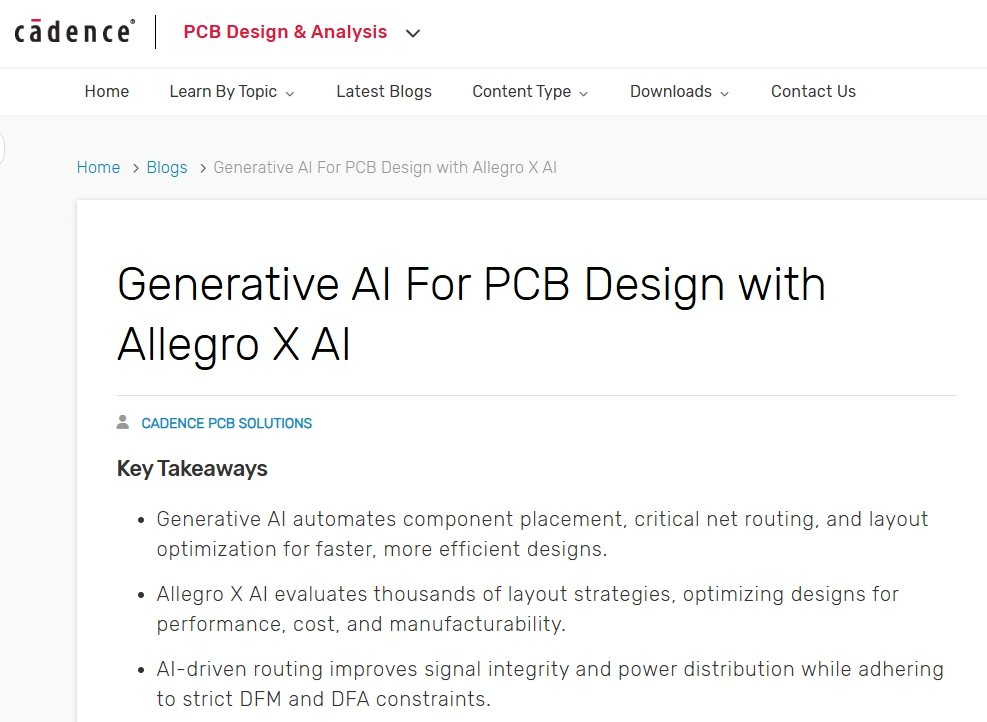
A published benchmark showed that Allegro X AI completed placement and routing tasks that traditionally took experienced designers three days in just 75 minutes, with a 12% improvement in total wire length. It automatically enforces DFA (Design for Assembly) and DFM constraints, meaning the routed designs are closer to fabrication-ready on the first pass.
The downside: Allegro is expensive, cloud integration is mandatory, and the learning curve is steep for teams accustomed to manual layout workflows. It’s built for large enterprises (aerospace, automotive, telecom) designing complex, high-reliability boards where the investment pays off.
Tool 3: DeepPCB (Cloud-Native AI Routing)
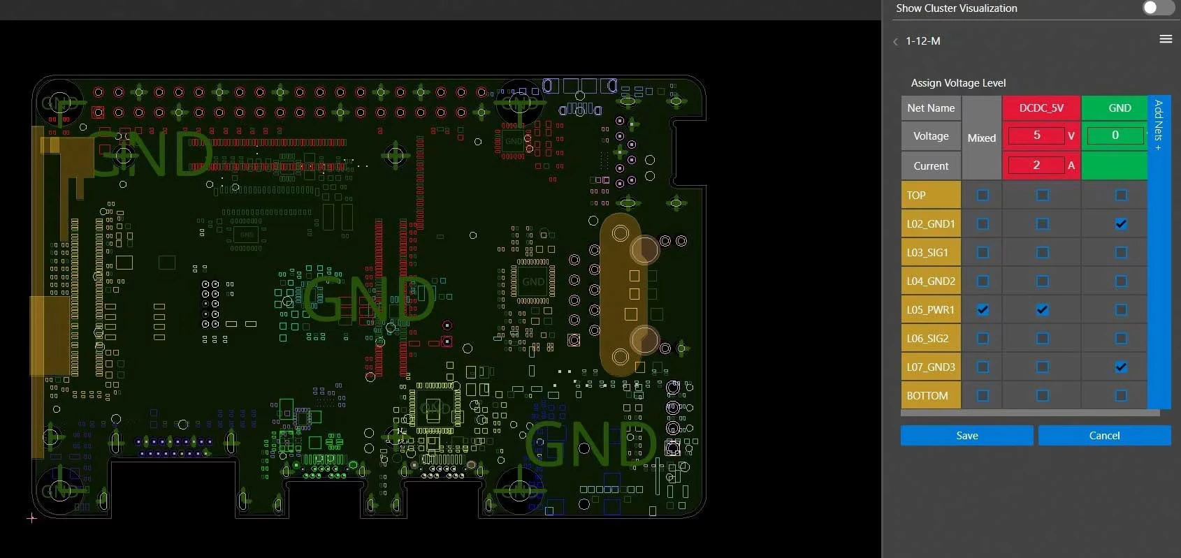
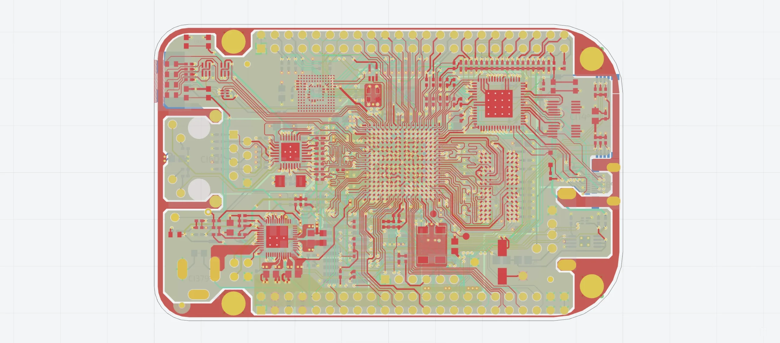
DeepPCB represents a different philosophy: pure AI, fully cloud-based, no legacy baggage. You upload your design files (KiCad, EasyEDA, Eagle, Altium), define a few constraints, and DeepPCB’s reinforcement learning engine generates a complete, DRC-clean layout in minutes. No graphical interface, no learning curve—just results.
The tool supports up to 8 layers, 1,200+ connections, blind/buried vias, and differential pairs. Importantly, it’s built on published research in combinatorial optimization and reinforcement learning, and it’s actively maintained by InstaDeep, a credible AI research firm.
Practical benefit for China manufacturing: DeepPCB outputs standard Gerber files and IPC-356 net lists, directly compatible with major Chinese PCB manufacturers. You don’t need to translate or clean up file formats.
The limitation: DeepPCB doesn’t offer interactive visual routing—you can’t “see” the design being routed in real time. Some designers find that uncomfortable. Also, it’s pay-per-design rather than a subscription, so costs scale with usage (typically $50–500 per design depending on complexity).
Tool 4: Flux with AI Copilot (Browser-Based, Collaborative)
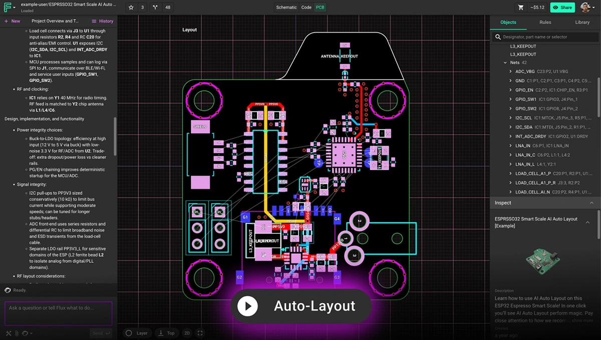
Flux is a browser-native ECAD platform designed for hardware startups and distributed teams. You design schematics and layouts directly in the browser (no installation), and Flux’s AI Copilot handles component placement and trace routing automatically, with real-time collaboration features built in.

Flux also integrates live component pricing and inventory data, so you can see supplier alternatives as you design. It supports multi-user editing—your colleague in Berlin can review your routing in real time while you’re working in San Francisco.
The trade-off: Flux is deliberately simplified compared to Altium or Cadence. It handles standard digital and analog designs well, but advanced features like fine-grained differential pair tuning or exotic stackups require manual work. That said, for teams shipping consumer IoT devices or wearables in 4–8 layers, Flux’s speed and ease of use are compelling.
Pricing is transparent: $15–49/month depending on tier, plus AI credits for routing jobs. That’s accessible for startups.
Tool 5: Quilter (Physics-Driven Autonomous PCB Layout)
Quilter claims to be the “first and only” physics-driven AI for PCB layout. Rather than learning from human-designed boards, Quilter trains on first-principles physics—Maxwell equations for electromagnetism, heat transfer equations, signal propagation models. The result: an AI that can discover routing solutions no engineer would consider because they defy intuition.

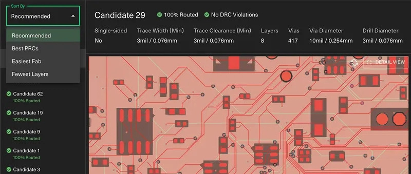
In practice, Quilter’s process works like this: You upload your schematic and design constraints. Quilter generates dozens of complete, physically validated layout candidates in parallel, each with different placement and routing strategies. You review the candidates, compare their electrical and thermal performance, and export your chosen design back to native Altium/Cadence/KiCad for final touches.
The promise is that Quilter eliminates weeks of manual PCB layout. Early customers (aerospace contractors, automotive Tier-1 suppliers) report significant cycle time compression.
The honest caveat: Quilter is early-stage and most effective on boards where component placement flexibility exists. If your mechanical constraints or connector locations are fixed, Quilter offers less advantage. Also, it doesn’t handle pure schematic capture or simulation—you still need your main EDA tool for those tasks.
Tool 6: Keysight EDA with AI/ML Optimization
Keysight‘s approach is more simulation-centric. Rather than automating routing directly, Keysight’s AI/ML features build surrogate models of circuit behavior using machine learning. These models train on your simulation data, then predict performance (signal integrity, power delivery, thermal) for candidate layouts very quickly—much faster than running full simulations.
This is particularly useful for RF and high-speed designs where simulation-driven optimization is essential. You can let AI explore thousands of layout variations and rank them by predicted performance, then route the top candidates manually or with assistance.
Best fit: Companies designing complex analog, RF, or power electronics where simulation dominates the workflow.
Tool 7: KiCad with AI Automation (Open-Source Path)
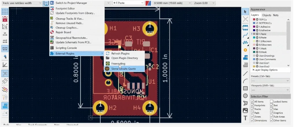
KiCad is open-source and free, but historically lacked a sophisticated autorouter. That’s changing. Several projects now layer AI on top of KiCad via Python scripting. Autocuro and Huaqiu (a Chinese EDA team) have published AI routing automation for KiCad that achieves placement and routing in ~10 minutes, plus ~3 hours of refinement—comparable to commercial tools.
The approach is pragmatic: parse the KiCad schematic file directly (not just the netlist) to extract design intent, use that context to guide placement and routing, and output DRC-compliant results.
Advantages: Free base tool, IP stays on your computer (no cloud upload), and it’s actively developed. Disadvantages: No commercial support, and results currently require more manual cleanup than Flux or DeepPCB.
This is ideal for academic teams, startups bootstrapping hardware, or open-source projects.
Tool 8: Autodesk Fusion 360 with Eagle (Mechanical-Electrical Integration)
Autodesk Fusion 360 (formerly known as Eagle when standalone) is cloud-based ECAD with strong integration into Autodesk’s mechanical CAD and simulation tools. If your hardware includes mechanical enclosures, thermal analysis, or parametric design relationships, Fusion 360’s unified environment is compelling.
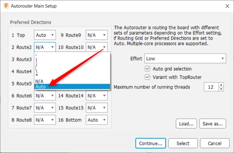
The PCB routing features include batch autorouting (multiple strategy variants), interactive routing with real-time constraint feedback, and differential pair support. It’s not as advanced as Allegro X AI, but it’s more approachable for teams balancing electrical and mechanical workflows.
Practical note: Fusion 360 is free for personal use, $460/year for startups, and custom pricing for enterprise. Ideal for makers, small teams, and companies doing product design (not just layout).
Tool 9: Zuken (Advanced PCB Layout and Optimization)
Zuken offers enterprise-grade PCB design solutions (such as CR-8000) with powerful constraint-driven routing and optimization capabilities. It focuses heavily on complex, multi-board and high-speed designs, providing advanced features for timing, signal integrity, and power integrity constraints.

You can highlight that Zuken’s environment supports:
- Intelligent auto and interactive routing based on detailed design rules and constraints.
- Layout optimization for high-speed buses, differential pairs, and dense BGA breakout.
- Tight integration between schematic, PCB, and system-level design, suitable for large teams and complex projects.
Best for: Large enterprises and teams handling complex, multi-board, high-speed systems who need deep constraint management and integration into broader system design and PLM workflows.
Tool 10: General-Purpose GenAI Assistants (ChatGPT, Claude, Gemini)
While ChatGPT and similar large language models can’t route a PCB directly, they’re surprisingly useful around the PCB workflow. You can use them to:
- Generate structured design rule sets in seconds for your EDA tool
- Create Python scripts to automate repetitive CAD tasks
- Draft Design for Test (DFT) checklists, reviewing your design against industry best practices
- Explain why a particular routed design violates signal integrity and suggest fixes
For teams without dedicated PCB design expertise, ChatGPT can act as a knowledgeable colleague, quickly filling knowledge gaps and accelerating learning.
How to Integrate AI Auto Routing into a Real PCB-to-PCBA Workflow
Theory is useful, but results matter. Here’s a step-by-step process for integrating AI routing into a genuine hardware development cycle that culminates in production in a Chinese PCB and PCBA factory.
Step 1: Choose Your AI Tool and Validate Compatibility.
Start by evaluating which tool fits your budget, team skills, and design complexity. If you’re already in Altium, stay there for continuity. If you’re budget-constrained and open-minded, try DeepPCB or Flux on a non-critical board first. Download or access the tool, route a simple test board, and confirm that the output file formats (Gerber, ODB++, drill files) are recognized by your EDA software and your target PCB manufacturer’s online platform.
This is important: Many Chinese PCB manufacturers accept Gerber RS-274X, Excellon drill files, and IPC-356 netlists. Confirm this before committing to a tool.
Step 2: Define Design Rules and Manufacturing Constraints Early.
Before you touch the AI router, sit down with your PCB manufacturer’s design guidelines. What is their minimum trace width? Spacing? Via diameter? Annular ring requirements? Layer count capabilities? Can they handle differential impedance control? Do they support blind/buried vias, microvias, or are they limited to through-hole vias?
Input these constraints into your AI tool’s constraint database. Most professional tools (Altium, Cadence, Allegro X AI) accept rule files or database entries. Cloud platforms (DeepPCB, Flux, Quilter) ask for these constraints upfront during the upload process.

Step 3: Prepare Your Schematic and Netlist Carefully.
Garbage in, garbage out. Before you route anything, perform a thorough schematic review. Verify:
- All power and ground connections are complete
- Component footprints match actual PCB pads (check datasheets for QFN, BGA orientation)
- Critical signals are identified and marked (high-speed clocks, differential pairs, analog references)
- No floating nets or typos in component names
Export a clean netlist. If you’re using Altium, use the built-in netlist export. KiCad users: generate a KiCad NETLIST file. DeepPCB and Quilter accept native design files.
Step 4: Run the AI Router and Generate Multiple Candidates.
Depending on your tool, this might take 5 minutes (DeepPCB, Flux) or 30 minutes (Allegro X AI evaluating thousands of strategies). Some tools, like Quilter, generate multiple design candidates automatically; others produce a single result.
If you get multiple candidates, take time to compare them. Allegro X AI and Quilter provide performance metrics (total wire length, via count, maximum trace delay, thermal hot spots). Choose the candidate that best aligns with your priorities. Often, the fastest design isn’t the cheapest to manufacture, and the most optimized wire length might use more vias than your budget allows.
Step 5: Review and Refine with Your Engineering Team.
Never trust the AI output blindly. Even sophisticated tools make mistakes. Your job is to:
- Visually inspect the routed design, layer by layer
- Verify that high-speed differential pairs are correctly spaced and length-matched
- Check that power and ground planes have adequate copper and no suspicious gaps or bottlenecks
- Confirm that vias aren’t clustered in a way that will stress the PCB during thermal cycling
- Ensure that traces don’t run under components (bad for rework and EMI)
- Look for any “wire rats nests” or unrouted connections
Most tools provide interactive editing: you can manually adjust traces if needed. Spend 2–4 hours here, depending on board complexity.
Step 6: Run Comprehensive DRC and DFM Checks.
Before you export, run your EDA tool’s Design Rule Check and, if available, a DFM analysis against your manufacturer’s constraints. This catches issues like:
- Trace width violations
- Insufficient clearance to board edge
- Via count or distribution that stresses the drill process
- Annular ring size violations on fine-pitch BGAs
- Solder mask coverage problems
Fix any yellow warnings. Altium and other mature tools can catch these issues automatically; simpler tools may require manual inspection against a DFM checklist (use ChatGPT to generate one quickly).
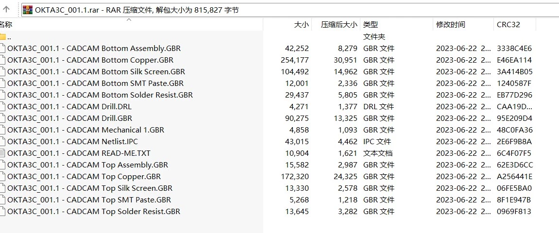
Step 7: Export Standard Manufacturing Files.
Generate the full manufacturing package:
- Gerber files: One for each copper layer (signal, plane), one for solder mask, one for silkscreen, one for board outline (typically 10–15 files total for an 8-layer board)
- Drill file: Excellon format, specifying hole diameters, plating (PTH vs NPTH), and coordinates
- BOM (Bill of Materials): Component designator, part number, value, package, quantity
- Pick & Place file: X-Y coordinates and rotation for each component
- IPC-356 netlist (optional but useful): For the manufacturer to verify continuity
Step 8: Prepare Documentation and Send to Manufacturer.
Create a design package that includes:
- All Gerber/drill files (zipped or tarred)
- BOM in CSV or Excel format, preferably with manufacturer part numbers (MPN) and preferred distributors (e.g., Digi-Key, Mouser, Heilind, Win Semiconductors for Asian sourcing)
- Pick & Place file
- Stack-up drawing (layer order, copper thickness, dielectric thickness, prepreg specifications)
- Notes on any special requirements (e.g., “Route DDR3 differential pairs on Layer 3–4 as stripline with 50-ohm impedance”)
Send this to your PCB manufacturer’s technical team. Many Chinese factories have free design reviews; use this service. They’ll spot issues you missed and suggest DFM improvements before you commit to fabrication.
Step 9: Review Manufacturer Feedback and Iterate if Needed.
The manufacturer might flag issues like:
- “Your annular ring on the BGA is too small; we recommend 6 mil minimum but you have 5 mil”
- “Differential impedance controlled to ±5% requires advanced layer stackup; standard FR-4 stackup achieves ±10%”
- “Your via-in-pad design requires tenting or filling; this adds $500 to the NRE.”
Work with them to resolve these. It’s much cheaper to fix the design now than to discover problems in production or during rework.
Step 10: Lock Design and Move to Production.
Once manufacturer feedback is addressed, formally release the design. Order a small batch (5–25 boards) as a first article inspection (FAI) prototype to verify that the AI routing worked in the real world. Check for cold solder joints, signal integrity on high-speed nets (use an oscilloscope if available), and thermal performance under load.
If the FAI passes, scale to production quantities.
Common Pitfalls of AI Auto Routing and How to Avoid Them
Even with the best tools, mistakes happen. Here are the most frequent problems and how to sidestep them.
Pitfall 1: Over-Relying on AI Without Design Context.
AI tools don’t understand your application’s purpose. They don’t know if the board will run in a car engine bay (high-temp, vibration) or a consumer smartphone (thin, competitive cost). They can’t read your system architecture document or know which signals are timing-critical.
Solution: Always provide explicit constraints. Mark critical nets. Define differential pair requirements. Set thermal derating limits if your device has power constraints. Most AI tools accept these inputs, but it’s your job to provide them. Take 30 minutes to write a constraint specification before you route.
Pitfall 2: Ignoring Differential Pair and High-Speed Requirements.
Even modern AI tools sometimes struggle with differential pairs on complex boards. They might generate pairs that are far apart on different layers, breaking coupling, or they might not length-match them to the required precision (e.g., ±5 mils for 6 Gbps USB 3.0).
Solution: For differential signals, define net classes in your EDA tool. Group USB DP/DM, PCIe lanes, DDR3/DDR4 signal pairs into explicit net classes with spacing and length matching rules. Then let the AI route. Afterward, visually inspect every differential pair and verify coupling and length. If the AI result is marginal, route those critical pairs manually.
Pitfall 3: Excessive Vias and Layer Bloat.
Naive AI routers sometimes generate more vias than necessary, as if vias were free. In reality, each via costs money (especially on high-layer-count boards) and introduces a potential failure point during thermal cycling. Some AI tools optimize for “completion speed” rather than “manufacturing cost.”
Solution: After AI routing, do a post-routing optimization pass. Tools like Altium’s interactive router let you consolidate vias, group vias in regular grids (better for automated drilling), and redistribute routing across layers more evenly. Aim for a via count that’s perhaps 20% higher than a skilled manual router would achieve, not 50% higher.
Pitfall 4: Forgetting the Big Picture: Power Delivery and Ground Planes.
AI routing focuses on signal traces, but a good PCB design is 50% power delivery and grounding. If your AI router fills the board with signal traces but leaves inadequate space for power planes or ground pour, the result will have noise and poor EMC performance.
Solution: Before running the AI router, block out areas of the board for power planes and solid ground planes. Define these constraints in your EDA tool so the AI respects them. Typically, Layers 2 and 5 (in an 8-layer board) are reserved for ground, Layers 3 and 6 for power planes, leaving Layers 1, 4, 7, 8 for signals. That’s a good starting point; adjust to your design’s needs.
Pitfall 5: Assuming One Routing Solution is Optimal.
You may use AI to generate a single routing, declare it “done,” and send to manufacturing. In reality, that one solution might be suboptimal for cost, signal integrity, or thermal performance.
Solution: Tools like Allegro X AI and Quilter inherently generate multiple candidates. If your tool generates only one, ask yourself: Could I route this differently? Could I use fewer layers? Could I concentrate vias differently? Take 30 minutes to manually explore 2–3 alternative routing strategies, compare their cost and performance, and pick the best. This extra effort often saves money downstream.
Pitfall 6: Skipping the Manufacturer Review.
You AI-route a board, generate Gerber files, and send directly to fabrication without manufacturer input. The factory’s DFM system catches your design’s inadequacies and flags an expensive re-spin.
Solution: Always invite your PCB manufacturer to review your design before you commit to production. Most Chinese PCB factories offer free design reviews (as a service to customers). Use this. They’ll spot manufacturing-specific issues (layer stackup mismatch, via size incompatibility, solder mask coverage risks) that your EDA tool doesn’t know about.
How IWDF Solutions Uses AI-Assisted Routing to Deliver Better PCB and PCBA Projects
As a Shenzhen-based PCB and PCBA manufacturer, IWDF Solutions understands the full spectrum of hardware design and production. We work with customers who arrive with complete designs (some using AI routing tools, some hand-routed) and others who need design-for-manufacturability optimization before production begins.
Here’s how we integrate AI-assisted design into our workflow:
Design Intake and Compatibility Review.
When you submit your PCB design files (whether they’re from Altium, KiCad, Cadence, or AI platforms like DeepPCB or Flux), our engineering team first verifies file integrity and compatibility with our manufacturing systems. We check Gerber layer naming, drill file format, and stackup specifications. If your design was AI-routed, we specifically look for DFM compliance: via size, annular ring, trace width distribution, and signal plane integrity.
We’ve worked with designs routed by every major AI tool mentioned in this article. We know which tools produce manufacturing-ready outputs (DeepPCB, Altium, Allegro X) and which typically require cleanup (KiCad automation, early Flux designs). We never hold this against a customer; instead, we proactively flag issues and offer optimization suggestions.
DFM Analysis and Optimization.
Using our in-house design analysis tools, we run a comprehensive DFM report on your routed design. This covers:
- Via size distribution: Are all vias in the 0.3–0.4 mm range (standard), or do you have a mix that complicates tooling?
- Trace width and spacing: Will your narrowest traces be within our process window (typically 0.1 mm ± 0.05 mm)?
- Annular ring: Are your BGAs and fine-pitch components compliant with IPC-A-600 Class 3?
- Impedance control: If you’ve specified controlled impedance traces (differential pairs, clock routes), do your layer stackup and trace geometry support the required tolerance (±10% or ±5%)?
- Solder mask coverage: Are there any micro-vias or fine traces at risk of solder mask bridging?
Our design engineers then prepare an optimization report. Often, we can reduce cost by 10–15% through intelligent DFM tweaks: consolidating vias, widening non-critical traces, or rebalancing layer usage. We never modify your critical signal paths without your approval.
Support for AI Tool Hand-Off to Manufacturing.
Many of our customers use cloud-based AI routing platforms like DeepPCB or Quilter. These tools generate excellent Gerber files but, by design, operate outside the traditional EDA environment. We’re comfortable receiving and validating these outputs.
If you’ve routed with DeepPCB and want to adjust a few traces or add test points, you have two options: (1) upload the Gerber back into your original EDA tool (Altium, KiCad, etc.) for modifications, then regenerate Gerbers, or (2) ask us to make minor adjustments during our DFM review and provide you with an updated design. We often do (2) for small changes, as it speeds time-to-fab.
PCBA Assembly Coordination.
Here’s where AI-routed designs sometimes need attention. If your AI router didn’t optimize component placement for assembly accessibility, our PCBA team might flag concerns:
- “Your BGAs are 4 mm apart; our pick-and-place can handle this, but it slows cycle time.”
- “Test points for your high-speed differential pairs are on Layer 2 (internal); we recommend adding accessible test points on the top or bottom surface.”
- “Your thermal pads for this power IC don’t have stitching vias in the 0.2 mm grid we typically use; this affects thermal performance.”
Again, we don’t reject designs; we explain trade-offs. You decide whether to optimize or accept the constraints.
From Design to Prototype and Production.
Once DFM is cleared, we prepare a production panel, tool the press/router, run a first article inspection (FAI), and move to your desired volume—whether that’s 5 units, 500, or 50,000. We manage supply chain and component sourcing, helping you navigate China’s electronics markets to find the best price-quality-lead-time trade-offs.
For teams new to China manufacturing, we also coordinate with your quality team: providing sample inspection reports, thermal and vibration testing data (if your design warrants it), and long-term reliability feedback from field deployments.
Our Commitment to Your AI Workflow.
To be direct: IWDF Solutions doesn’t view AI-routed designs as “lesser” or requiring extra scrutiny. We view them as a natural evolution of PCB design. What we do require is that your design, whether hand-routed or AI-assisted, arrives with clear documentation of constraints, intent, and any non-standard requirements. That transparency lets us deliver your boards efficiently and to the quality standard your application demands.
If you’re evaluating AI routing tools and want to see how your design translates to production, send us a sample Gerber set (sanitized if confidentiality is a concern). We’ll run a free preliminary DFM review, point out any manufacturing-specific issues, and give you an honest assessment of production feasibility and cost. It’s part of how we help customers succeed.
Frequently Asked Questions About AI Auto Routing in PCB Design
Q: Will AI auto routing make skilled PCB designers obsolete?
A: No. AI tools automate the mechanical, repetitive aspects of routing—connecting nets, avoiding collisions, balancing layer usage. But they can’t understand your product’s purpose, anticipate edge cases, or make creative trade-offs between cost, performance, and schedule. A PCB designer in 2026 is evolving from “person who manually traces every connection” to “an engineer who sets strategy, reviews AI output, and handles exceptions.” That’s still a high-skill, high-value role. Companies that combine AI tools with experienced designers will win.
Q: Can AI routing replace traditional EDA tools like Altium or Cadence?
A: Not fully, but they complement each other. If you’re designing a one-off prototype, a standalone cloud tool like DeepPCB is faster than learning Altium. But if you’re managing a design team with hundreds of projects, a mature EDA platform like Altium (with AI-assisted features) gives you consistency, library control, and long-term maintenance benefits. Think of it this way: Altium is a “design operating system”; AI routing is a “specialized plugin.” You need both for a complete flow.
Q: How much does AI routing actually save in time and cost?
A: For prototypes and simple boards, savings are dramatic: 70–80% reduction in routing time (from 1–2 days to 2–4 hours). For complex, high-density boards, savings are more modest: 30–50% (from 5 days to 2–3 days), because more manual optimization and engineering judgment is needed. In dollars, if your loaded cost for an engineer is $100/hour, then 10 hours saved per design is $1,000 in labor. That’s meaningful for high-volume design shops or competitive markets. For one-off products, the time savings matter more than the cost savings—faster time-to-market can be worth millions in revenue opportunity.
Q: What about signal integrity? Does AI routing understand high-speed design?
A: Modern AI tools understand signal integrity in principle—they know about differential pair spacing, impedance control, length matching, return paths. But they can’t simulate the full electromagnetic effects the way a dedicated SI analysis tool can. The workflow is: let AI do initial routing, then simulate signal and power integrity using Ansys or AltiumSI, identify problems, and let the engineer make targeted fixes. AI doesn’t replace SI simulation; it speeds up the initial design phase.
Q: Can I use an AI-routed design from one tool in another EDA platform?
A: Yes, if you export to Gerber (and drill files). A Gerber file is a manufacturing format, not an EDA-specific format. You can take Gerbers from DeepPCB, import them into Altium Designer for further editing, and export new Gerbers. The limitation: re-importing Gerbers into your EDA tool loses some metadata (net names, component references), so future edits are harder. Best practice: if you might need to make changes later, keep the original design files (.kicad_sch, .sch, .eda) and regenerate Gerbers after edits, rather than editing Gerbers directly.
Q: Is AI routing suitable for high-volume manufacturing in China?
A: Absolutely. In fact, Chinese manufacturers are increasingly comfortable with AI-routed designs. The key is ensuring DFM compliance and clear documentation. Chinese factories are highly optimized for cost and speed; they don’t care whether your design was routed by a human in California or an AI in the cloud, as long as the Gerbers are correct and your BOM is clear. We at IWDF Solutions handle AI-routed designs regularly. The main difference in our process is that we spend an extra hour in DFM review to validate that the AI’s routing choices are compatible with our specific process window. That’s a one-time cost that ensures smooth production.
Q: What’s the biggest risk when using AI routing?
A: The biggest risk is over-trusting the AI and under-reviewing the output. AI routing is fantastic for 85–90% of your board, but the remaining 10–15% often includes critical paths where engineering judgment is essential. Power distribution, high-speed differential pairs, thermal hotspots—these warrant manual inspection and, if needed, manual adjustment. Also, AI tools can’t account for unique constraints specific to your application (e.g., “This board will vibrate 10 Gs continuously; vias in this zone must be in a regular grid for vibration tolerance”). Make sure you explicitly feed such constraints into the tool upfront.
Q: Which AI routing tool should I choose?
A: It depends on your situation. If you’re already in Altium or Cadence, upgrade to the latest version and use their built-in AI features—minimal disruption. If you’re starting fresh or bootstrapping a startup, try Flux or DeepPCB (both have free trials or low cost-of-entry). If you’re designing complex aerospace or automotive hardware, investigate Allegro X AI or Quilter—the investment pays off through superior optimization. If you’re in academia or open-source, use KiCad + AI automation. There’s no universal “best” tool; there’s the best tool for your constraints and workflow.
Q: Do I need to worry about intellectual property if I use a cloud-based AI tool?
A: Some cloud tools (like Quilter) explicitly promise not to use your design data for AI training. Others don’t guarantee this. If IP confidentiality is critical, ask the tool vendor directly in writing. Alternatively, use on-premise or local tools (Altium, KiCad with AI plugins) where your design never leaves your computer. For most commercial products, the risk is low; for cutting-edge proprietary designs, it’s worth a conversation with your legal team.
Q: How do I prepare my design for AI routing to maximize quality?
A: (1) Clean schematic: verify all connections, check footprints, and fix any errors before export. (2) Define net classes: explicitly mark high-speed nets, differential pairs, power/ground. (3) Set constraints: input layer stackup, trace width/spacing rules, impedance targets, via size limits. (4) Provide notes: document any special requirements (thermally sensitive components, EMI shielding zones, mechanical constraints). (5) Review manufacturer capabilities: know the PCB factory’s process window and input those limits into the tool. (6) Generate multiple candidates: if the tool supports it, ask for 3–5 routing options and compare them. Following these steps, your AI routing will be 95%+ production-ready on the first pass.
Conclusion: AI Auto Routing Is Here, and It’s Good (When Used Right)
AI-powered PCB auto routing has matured from a curiosity to a legitimate productivity tool. The best tools today—whether Altium’s integrated AI, Cadence’s generative Allegro X AI, or physics-driven platforms like Quilter—save significant time without sacrificing quality, provided you use them thoughtfully.
The workflow is no longer “manually route everything” or “blindly trust the autorouter.” It’s “let AI handle the repetitive work, you focus on strategy and validation.” For hardware teams in Europe, the US, and Asia, that shift is reshaping how PCBs get designed and brought to market.
If you’re evaluating AI routing tools and considering production in China, you have a partner in IWDF Solutions. We understand both the AI design workflows and the manufacturing realities of Chinese PCB and PCBA production. We’ve reviewed designs from every major AI tool, optimized them for DFM, and shipped production boards that met or exceeded our customers’ performance and reliability targets.
Whether your design was routed manually, semi-automatically, or fully by AI, we’re here to validate, optimize, and manufacture it reliably. Send us your design files, your BOM, and your production requirements. Our engineering team will review DFM, identify any manufacturing-specific issues, and provide an honest assessment of production cost, lead time, and quality outlook.
The future of PCB design is collaborative: human engineers setting strategy, AI tools executing the mechanical work, and experienced manufacturers validating and realizing the physical design. That’s the model we embrace at IWDF Solutions, and it’s the model we recommend to any team serious about getting high-quality hardware to market fast.
About IWDF Solutions
IWDF Solutions is a Shenzhen-based PCB design and manufacturing partner providing one-stop PCB design, prototyping, and PCBA services. We serve hardware teams globally, from startups shipping their first product to established OEMs scaling production. We work with designs in every state—from schematic review, through layout optimization, to full production and quality assurance. Whether you’re using traditional EDA tools or the latest AI routing platforms, we’re equipped to review, optimize, and manufacture your designs to world-class standards.

