
5G Smart Mobile Phone PCB Design and HDI Manufacturing Case Study.
A complete smartphone PCB design and engineering case based on the MTK Dimensity 7050 platform, developed with production, certification, and OEM scalability in mind.
- 5G mobile PCB architecture & layout
- RF, power & high-speed signal optimization
- Design aligned with certification and mass production
- Prototype validation to production-ready PCB

Project Overview
This project showcases the design and engineering process behind a 5G smartphone built with the MediaTek MT6877 (Dimensity 7050) chipset. Leveraging an advanced 6nm process and an octa-core 2.4GHz CPU, the device delivers exceptional efficiency for communication, imaging, and data handling.
The phone supports global 5G bands and offers flexible configuration options for dual Nano-SIM and TF cards, making it an adaptable solution for worldwide deployment. With a solid, rugged structure, IP68 waterproofing, and reversible assembly, it meets the demands of outdoor, industrial, and premium applications alike.
The Real Challenge in 5G Mobile OEM Projects
For OEM clients, 5G smartphone projects rarely fail because of missing features.
They fail because critical hardware decisions are locked before production realities are fully understood.
When PCB design moves faster than RF validation, testing strategy, and certification planning, problems surface late—when changes are most expensive and timelines are already under pressure.
- RF behavior is defined too late Layout choices delay tuning, stability verification, and network performance validation.
- Testing and certification paths are unclear Missing test access and validation planning lead to repeated board revisions.
- Late-stage PCB changes block production readiness Once layout is frozen, even small fixes can delay pilot builds and mass production schedules.
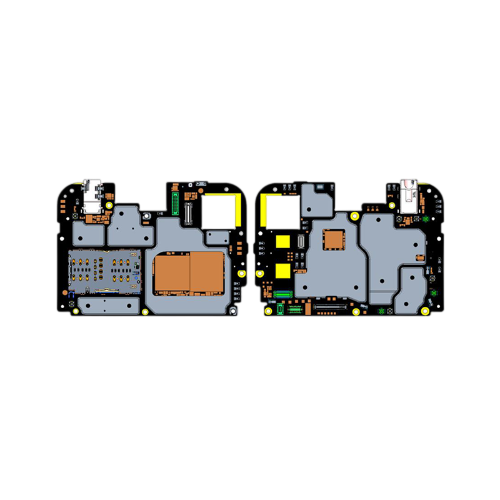
Designing the PCB for Manufacturability from Day One
Instead of treating PCB design as a standalone task, this project approached it as a production-bound system. From the earliest design stage, the PCB was developed with manufacturing flow, validation processes, and certification timelines already in mind—so design decisions would accelerate, not delay, downstream execution.
- 5G RF routing planned with isolation and tuning margins. RF zones and return paths were defined early to reduce rework during validation.
- High-speed signal integrity under dense component placement Stack-up and routing strategies balanced performance with assembly yield.
- Power delivery designed for peak 5G transmission loads. Power planes and decoupling were optimized to maintain stability under real operating conditions.
- Thermal behavior considered within a compact enclosure. Layout decisions accounted for heat dissipation before mechanical integration.
- Test-friendly layout for validation and certification. Test points and probing access were incorporated to support efficient compliance testing.
From PCB Design to a Market-Ready Device
Transforming an advanced idea into a fully operational 5G smartphone requires a seamless transition from concept to production. In this project, our engineering team led the complete journey — starting from PCB architecture design and component placement optimization to firmware debugging, mechanical integration, and reliability verification. Each design iteration focused on achieving high signal integrity, efficient heat dissipation, and robust performance under global 5G conditions. Through continuous cross-functional collaboration, we bridged the gap between electronic design, structural engineering, and user experience.
The result is a market-ready device that integrates state-of-the-art hardware, intelligent software, and durable craftsmanship — a powerful demonstration of end-to-end innovation from PCB design to final product delivery.
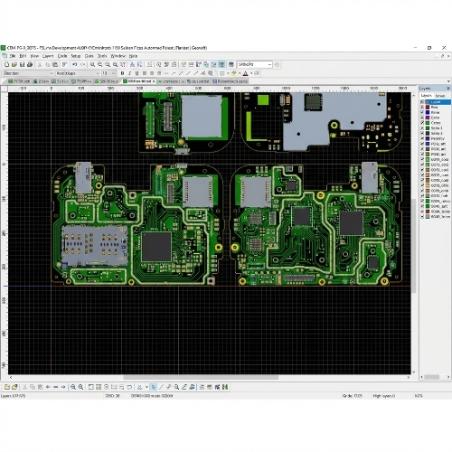
Smartphone PCB Design
PCB design started in parallel with core smartphone functions and industrial design. Component placement, routing strategy, and power distribution were defined to support processor performance, camera integration, display interfaces, and compact device thickness—without compromising electrical stability.

PCB Architecture
The PCB architecture translated functional and form-factor requirements into a repeatable, compliant structure. RF sections were organized to support required frequency bands alongside cameras and shielding, while stack-up and impedance control balanced signal integrity, EMI control, and manufacturability for CE and FCC compliance.
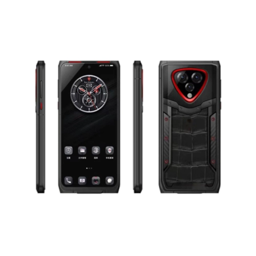
Market-Ready 5G Smart Mobile Phone
With functionality, appearance, and compliance aligned early, the device moved smoothly through RF validation, certification testing, and pilot production. Mechanical integration and assembly proceeded without major PCB redesigns, enabling a clear path to commercial deployment.
Reference Hardware Specifications
Platform & Performance
Chipset: MediaTek MT6877 (Dimensity 7050) CPU: Octa-core, up to 2.4 GHz Process: 6 nm Network: Global 5G bands, Dual 5G standby
Camera
Rear: 48 MP + 16 MP (Ultra-wide) + 8 MP (Macro) + 2 MP Front: 16 MP
Features
Fingerprint: Rear / Side Sensors: Gyroscope, NFC, G-sensor, light & proximity, optional barometer & temperature Audio: Smart amplifier, secondary mic noise reduction
Display
Size: 6.517" Resolution: HD+ (Support up to FHD+) Type: Waterdrop / corner blind-hole Panel: Incell / Oncell
Battery & Power
Capacity: 5000 mAh Charging: 18W fast charge, wireless charging, OTG
Mechanical
Protection: IP68 (selected models) Size: 165.3 × 78.7 × 14.6 mm
Technical Specifications
To meet the demanding requirements of 5G New Radio (NR) connectivity, this design integrates advanced High-Density Interconnect (HDI) architecture with specialized low-loss substrate materials. Our engineering approach focuses on maintaining precise signal integrity and robust thermal management within an ultra-compact mobile form factor. The following technical specifications represent the performance benchmarks achieved to ensure stable, high-speed data transmission and industrial-grade reliability for 5G smartphone applications.

1. Signal Integrity & Impedance Control
To support high-frequency 5G data transmission without distortion, our engineering team implemented rigorous impedance control strategies. We maintained a precise tolerance of plus or minus 10% across all critical paths. Specifically, RF signal traces were matched to a 50-ohm single-ended impedance, while high-speed digital pairs were meticulously calibrated to 100-ohm differential impedance, effectively eliminating signal reflections and ensuring seamless connectivity.
2. 5G MIMO Antenna Isolation
Integrating multiple antennas into a compact smartphone form factor presents significant electromagnetic interference (EMI) challenges. We utilized specialized shielding cans and strategic "ground fences" (via stitching) to achieve a port-to-port isolation of over 20dB. This optimized layout successfully reduced the Envelope Correlation Coefficient (ECC) to below 0.04, significantly enhancing the diversity gain and throughput of the 5G MIMO system.
3. Advanced Manufacturing & Testing
To accommodate the extreme density of 5G components, we employed Laser Drilling technology for ultra-fine microvias, enabling complex Any-layer HDI routing.
Our quality assurance process involves:
Automated Optical Inspection (AOI): Ensuring 100% accuracy in trace formation and component placement at a 0.3mm pitch.
Vector Network Analyzer (VNA) Testing: Rigorous validation of S-parameters to confirm that return loss and insertion loss meet the stringent requirements of mmWave and Sub-6GHz bands.
4. Compliance & Standards
This 5G smartphone PCB was designed and manufactured to meet the IPC Class 3 standard, ensuring the highest level of reliability for mission-critical mobile communication. The design is fully compliant with global regulatory requirements, including CE and FCC certifications, guaranteeing safety, performance, and international market readiness.
5G PCB Material Performance Comparison
| Material Type | Dielectric Constant (Dk) | Dissipation Factor (Df) | Frequency Range | Application Case |
|---|---|---|---|---|
| Standard FR-4 | 4.2 - 4.5 | 0.0200 | < 1 GHz | Digital & Control Circuits |
| High-Speed FR-4 | 3.6 - 4.0 | 0.0100 | 1 - 5 GHz | Sub-6GHz Digital Path |
| Rogers RO4350B | 3.48 | 0.0037 | 10 GHz+ | 5G RF Signal Path |
| Rogers RO3003 | 3.00 | 0.0010 | 28 GHz+ | mmWave Antenna Modules |
| PTFE / Low-Loss | 2.1 - 2.2 | 0.0009 | 77 GHz+ | 5G High-Frequency MIMO |
How We Control Quality in 5G Smartphone PCB Projects
Quality control embedded from design validation to production consistency.
- Design Intent Verification: Before layout freeze, PCB design was reviewed against RF performance targets, high-speed signal margins, power integrity limits, and EMI risk factors to ensure design intent was technically achievable and repeatable.
- Process & Material Consistency Control: Stack-up structure, laminate materials, copper thickness, and impedance targets were selected and locked based on both RF behavior and manufacturing capability to avoid performance drift between prototype and production builds.
- Assembly & Test Alignment: PCB layout incorporated test access and probing points to support RF validation, functional testing, and production-level verification, ensuring issues could be detected early and traced efficiently.
